Semiconductor device and semiconductor device manufacturing method

a semiconductor device and semiconductor technology, applied in the direction of semiconductor devices, basic electric elements, electrical appliances, etc., can solve the problems of deteriorating device characteristics affecting the performance of the semiconductor device, so as to improve the solder wettability, prevent bending stress being exerted, and improve the effect of solder wettability

Inactive Publication Date: 2012-12-13
FUJI ELECTRIC CO LTD
View PDF4 Cites 18 Cited by
  • Summary
  • Abstract
  • Description
  • Claims
  • Application Information

AI Technical Summary

Benefits of technology

[0025]The invention, in order to eliminate the problems of the heretofore known technology, provides a semiconductor device and semiconductor device manufacturing method that prevent breakage and chipping of a semiconductor chip. Also, the invention provides a semiconductor device and semiconductor device manufacturing method that prevent deterioration of device characteristics. Also, the invention provides a semiconductor device and semiconductor device manufacturing method whereby the device characteristics improve.
[0046]According to the invention, it is possible to worsen the solder wettability in at least the bottom surface and a bottom surface corner portion of the depressed portion. Because of this, at least the bottom surface and bottom surface corner portion (an eave portion) of the depressed portion are not joined to the circuit substrate by the solder layer. Consequently, even when the circuit substrate, or the like, expands due to a thermal shock, and stress is exerted on the substrate from the exterior, it is possible to prevent bending stress being exerted on the eave portion. Also, as it is possible to prevent bending stress being exerted on the eave portion, it is possible to prevent cracking and detachment occurring in the FP and passivation film provided on the eave portion.
[0047]According to the fifth aspect of the invention, the solder layer is provided in such a way as to cover a flat portion (flat portion) of the rear surface of the substrate and the side wall of the depressed portion. For this reason, the junction area of the substrate and, for example, the Cu base for cooling joined thereto across the circuit substrate increases in comparison with a semiconductor device in which the solder layer is provided on only the flat portion of the rear surface of the substrate, and it is possible to improve heat radiation.
[0048]According to the tenth to twentieth aspects of the invention, by making the thickness of the outermost electrode film of the electrode on the side wall of the depressed portion 0.05 μm or less, not forming the electrode on the bottom surface of the depressed portion, and forming a film covering the electrode on at least the bottom surface and bottom surface corner portion of the depressed portion, it is possible to worsen the solder wettability in the bottom surface and bottom surface corner portion of the depressed portion. Because of this, it does not happen in the joining step that the melted solder creeps up from the flat portion side of the rear surface of the substrate to the bottom surface of the depressed portion. Consequently, it is possible to form the solder layer in such a way that at least the bottom surface and bottom surface corner portion (the eave portion) of the depressed portion and the circuit substrate are not joined. Consequently, even when the circuit substrate, or the like, expands due to a thermal shock, and stress is exerted on the substrate from the exterior, it is possible to prevent bending stress being exerted on the eave portion.
[0049]According to the tenth, fifteenth, and eighteenth aspects of the invention, it is possible to form a film covering the electrode on the bottom surface and bottom surface corner portion of the depressed portion, and it is possible to form the solder layer in such a way as to cover the flat portion (flat portion) of the rear surface of the substrate and the side wall of the depressed portion. For this reason, the junction area of the substrate and, for example, the Cu base for cooling joined thereto across the circuit substrate increases in comparison with a semiconductor device in which the solder layer is provided on only the flat portion of the rear surface of the substrate, and it is possible to improve heat radiation.
[0050]According to the semiconductor device and semiconductor device manufacturing method according to the invention, an advantage is obtained in that it is possible to prevent breakage and chipping of a semiconductor chip. Also, an advantage is obtained in that it is possible to prevent deterioration of device characteristics. Also, an advantage is obtained in that it is possible to improve the device characteristics.

Problems solved by technology

Because of this, there is a danger of breakage or chipping occurring in semiconductor chip 100.
Because of this, there occurs a danger of the device characteristics of the semiconductor device deteriorating.
Because of this, there is a danger of the device characteristics of the semiconductor device deteriorating.

Method used


Image

  • Semiconductor device and semiconductor device manufacturing method
  • Semiconductor device and semiconductor device manufacturing method
  • Semiconductor device and semiconductor device manufacturing method

Examples


first embodiment

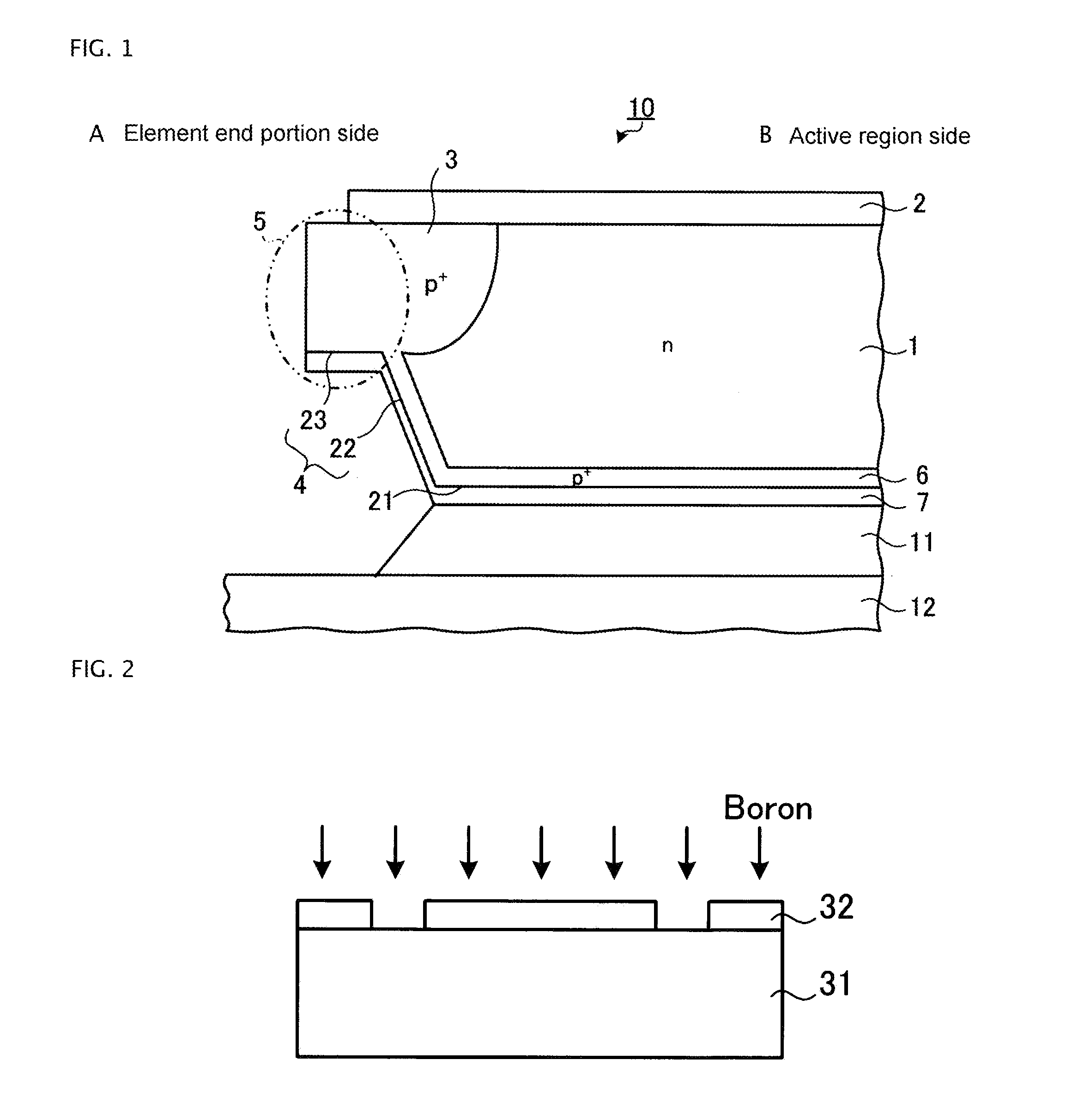
[0091]FIG. 1 is a sectional view showing a main portion of a semiconductor device according to a first embodiment. The semiconductor device shown in FIG. 1 includes semiconductor chip 10, and insulating substrate (a circuit substrate) 12 such as a ceramic insulating substrate (a DBC substrate). A reverse blocking type of semiconductor element having bidirectional voltage resistance characteristics is formed on semiconductor chip 10. Specifically, front surface element structure 2 is provided on the front surface (first main surface) of n-type (first conductivity type) drift region 1 formed from semiconductor chip 10.

[0092]A metal oxide semiconductor (MOS) gate structure configured of a p+-type base region, an n+-type emitter region, an emitter electrode, a gate electrode, and the like, is provided on an active region side (element central portion side) as front surface element structure 2. Also, a voltage resistant structure configured of a field limiting ring (FLR), which is a floa...

second embodiment

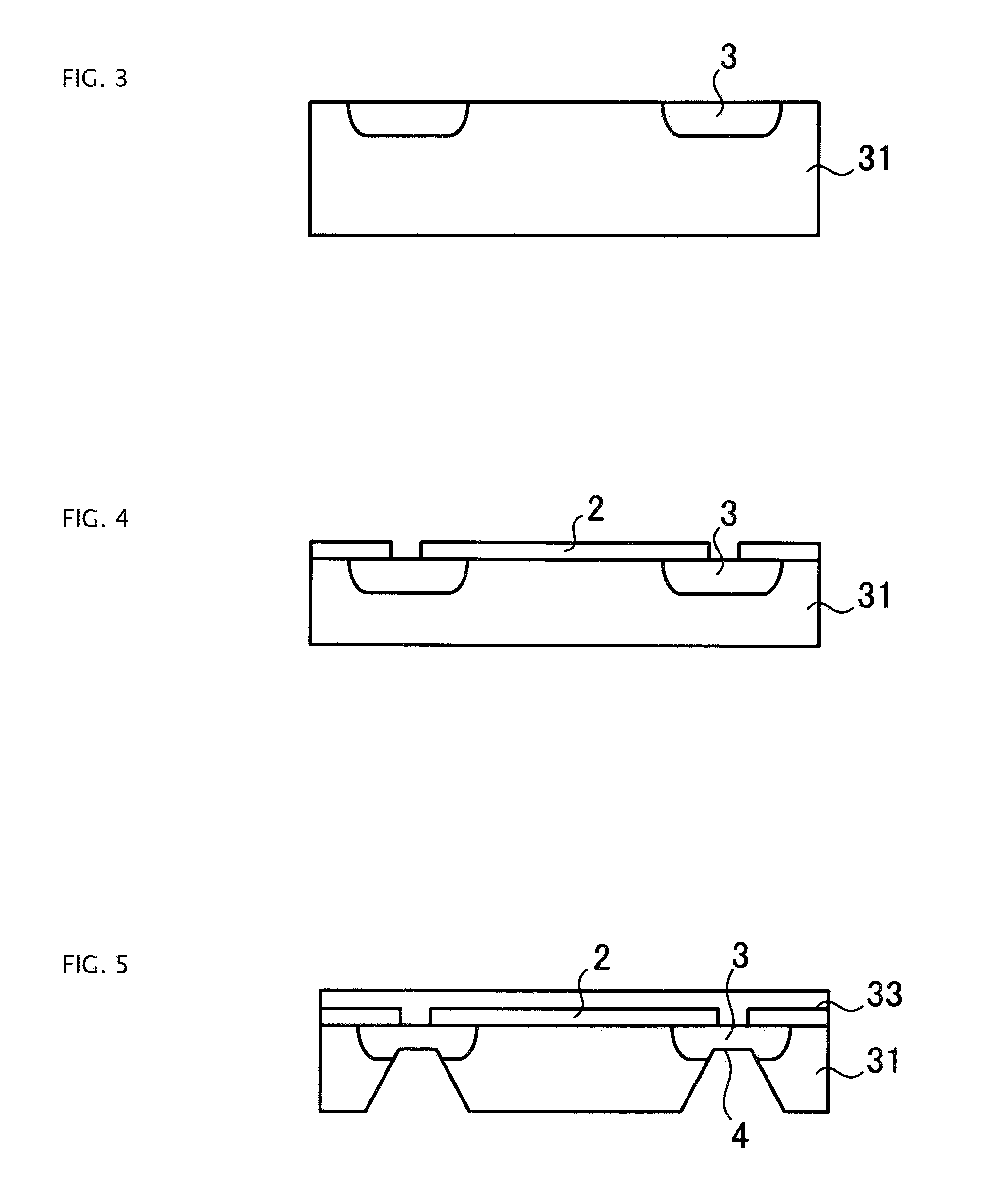
[0112]FIG. 10 is a sectional view showing a main portion of a semiconductor device according to a second embodiment. In the second embodiment, the configuration may be such that collector electrode 7 is not provided on bottom surface 23 of depressed portion 4.

[0113]In the second embodiment, as shown in FIG. 10, collector electrode 47 is provided extending from flat portion 21 of the rear surface of semiconductor chip 40 to side wall 22 of depressed portion 4. That is, collector electrode 47 is not provided on bottom surface 23 or bottom surface 23 corner portion of depressed portion 4. The thickness of collector electrode 47 may be a uniform thickness on both flat portion 21 of the rear surface of semiconductor chip 40 and side wall 22 of depressed portion 4, or the thickness on side wall 22 of depressed portion 4 may become gradually less from an open end portion side to bottom surface 23 corner portion of depressed portion 4. Also, collector electrode 47 may be a multilayer film.

[...

third embodiment

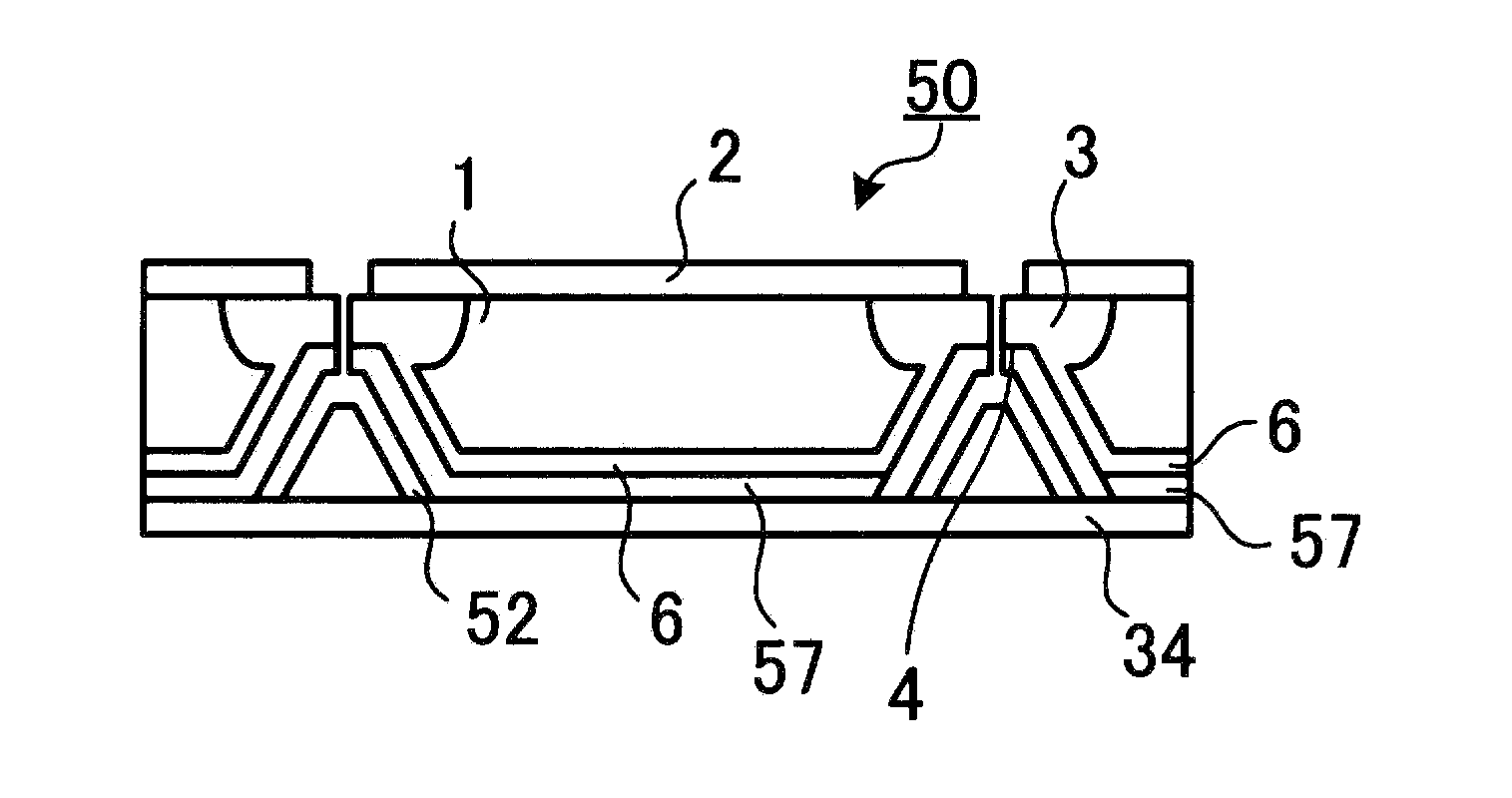
[0120]FIG. 13 is a sectional view showing a main portion of a semiconductor device according to a third embodiment. In the first embodiment, a configuration may be such that the collector electrode provided on side wall 22 and bottom surface 23 of depressed portion 4 is covered with a polyimide resin film.

[0121]In the third embodiment, as shown in FIG. 13, collector electrode 57 is provided extending from flat portion 21 of the rear surface of semiconductor chip 50 to bottom surface 23 of depressed portion 4. The thickness of collector electrode 57 may be a uniform thickness from flat portion 21 of the rear surface of semiconductor chip 50 to bottom surface 23 of depressed portion 4. Also, collector electrode 57 may be a multilayer film. Collector electrode 57 on side wall 22 and bottom surface 23 of depressed portion 4 is covered with film 52 formed from a material with poor solder wettability. Film 52 formed from a material with poor solder wettability may be, for example, a polyi...


PUM


Abstract

A semiconductor device and manufacturing method are disclosed which prevent breakage and chipping of a semiconductor chip and improve device characteristics. A separation layer is in a side surface of an element end portion of the chip. An eave portion is formed by a depressed portion in the element end portion. A collector layer on the rear surface of the chip extends to a side wall and bottom surface of the depressed portion, and is connected to the separation layer. A collector electrode is over the whole surface of the collector layer, and is on the side wall of the depressed portion. The thickness of an outermost electrode film is 0.05 μm or less. The collector electrode on the rear surface of the chip is joined onto an insulating substrate via a solder layer, which covers the collector electrode on a flat portion of the rear surface of the semiconductor chip.

Description

BACKGROUND OF THE INVENTION[0001]A. Field of the Invention[0002]The present invention relates to a semiconductor device and semiconductor device manufacturing method.[0003]B. Description of the Related Art[0004]A reverse blocking type of semiconductor element having bidirectional voltage resistance characteristics is commonly known as a power semiconductor element used in a power converting device or the like. With the reverse blocking type of semiconductor element, it is necessary to extend a p-n junction from the rear surface to the front surface of the semiconductor element in order to ensure reverse voltage resistance. In order to form the p-n junction extending from the rear surface to the front surface, a separation layer formed from a diffusion layer is provided in an element end portion of the semiconductor element.[0005]A reverse blocking type of semiconductor element in which a depression portion is provided in the rear surface of an element end portion, including a portio...

Claims


Application Information

Patent Timeline
Patent Type & Authority Applications(United States)
IPC IPC(8): H01L29/02H01L21/50H01L21/20
CPCH01L29/0619H01L29/0646H01L2924/3651H01L2924/3656H01L2924/0002H01L2924/00014H01L2924/01327H01L21/78H01L2924/10158H01L21/761H01L2224/94H01L2224/32227H01L2224/291H01L2224/29023H01L2224/26145H01L29/0657H01L29/0661H01L29/0692H01L29/0834H01L29/41741H01L29/41766H01L29/7395H01L2224/05012H01L2224/29024H01L21/76898H01L24/03H01L24/05H01L24/11H01L24/32H01L21/6836H01L2221/68327H01L2224/04026H01L2224/05008H01L2224/05124H01L2224/05548H01L2224/05562H01L2224/05573H01L2224/05644H01L2924/014H01L2224/03H01L2924/00H01L2224/05552H01L2924/351H01L2924/15747H01L2924/12042H01L2924/10156
Inventor FUKUDA, KYOHEIMOCHIZUKI, EIJISAWANO, MITSUTOSHISUZAWA, TAKAAKI
Owner FUJI ELECTRIC CO LTD
Why Eureka
Try Eureka