Method and system for providing automatic gate bias and bias sequencing for field effect transistors

a field effect transistor and gate bias technology, applied in the field of amplifiers with field-effect devices, electrical apparatus, high-frequency amplifiers, etc., can solve the problems of low gate bias voltage (vsub>g/sub>), drift of current (isub>d/sub>), and no one has fully solved the problem. , to achieve the effect of low cost, low power consumption and light weigh

Active Publication Date: 2012-12-13
EMHISER RES
View PDF3 Cites 33 Cited by
  • Summary
  • Abstract
  • Description
  • Claims
  • Application Information

AI Technical Summary

Benefits of technology

[0010]The present invention is intended for many uses and applications including in design and manufacture of airborne and ground-based telemetry equipment, including aircraft (manned and unmanned), ground vehicles, fixed systems and military telemetry equipment. Telemetry system components include transmitters, receivers, and power amplifiers in a wide variety of frequency ranges. As in many areas, there is a growing need and desire for telemetry components that are low cost, low power consumption (for battery, heat and other concerns), light weight, low failure rate, less complex, compact, more robust and rugged design for harsh environments, and of course high performance. For instance, the RF amplifier gate bias circuit of the present invention may be incorporated in transmitters, receivers, and power amplifiers.
[0013]In yet another aspect of the invention an advantage over prior circuits is that it does not attempt to minimize the spurious responses by better decoupling or improved grounding or any of the other known techniques. Rather, the circuit of the invention eliminates the problem entirely by shutting down the negative voltage deriving oscillator once it is no longer needed.
[0014]In a further aspect, the present invention provides an improved N-Channel depletion device-based amplifier with novel gate bias circuit and sequencer. With any N-Channel depletion device, such as GaAs FET, GaN FET, or N-channel silicon junction FET, it is essential that the negative gate voltage arrives before the drain voltage or the drain to source resistance is a very low value which will essentially short out the input power and likely cause damage to several circuit components including the depletion device. The present invention provides a novel sequencer for more effectively maintaining the necessary condition to prevent damage to amplifier components. The present invention may also provide an Adaptive Drain Current Control (ADCC). In a further aspect, an opto-coupler may be used in the circuit or in the alternative a battery or a Peltier Effect thermoelectric device.

Problems solved by technology

LDFETs also have a major disadvantage in that the gate bias voltage (Vg) required to set the quiescent current (Id) drifts over temperature, time, input drive, and frequency, as well as from device to device variations.
Considerable effort has been expended by the various manufacturers of these devices to lessen this undesirable effect, but no one has fully solved the problem.
With any N-Channel depletion device, such as GaAs FET, GaN FET, or N-channel silicon junction FET, it is essential that the negative gate voltage arrives before the drain voltage otherwise the drain to source resistance is a very low value which will essentially short out the input power and likely cause damage to several circuit components including the depletion device.
Existing approaches to sequencing for GaN devices, e.g., test fixture set up for fire-up and shut-down sequencing, are cumbersome and are external to the device, e.g., amplifier.

Method used


Image

  • Method and system for providing automatic gate bias and bias sequencing for field effect transistors
  • Method and system for providing automatic gate bias and bias sequencing for field effect transistors
  • Method and system for providing automatic gate bias and bias sequencing for field effect transistors

Examples


Embodiment Construction

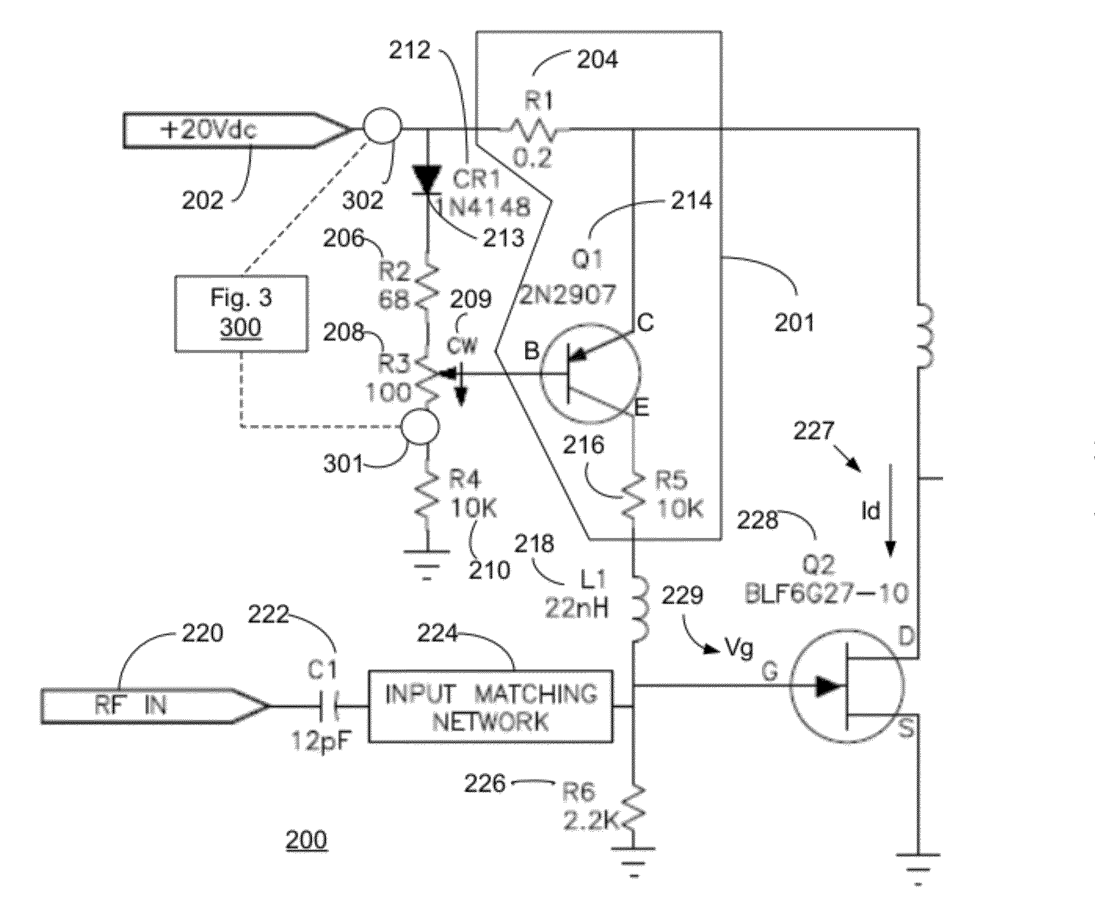
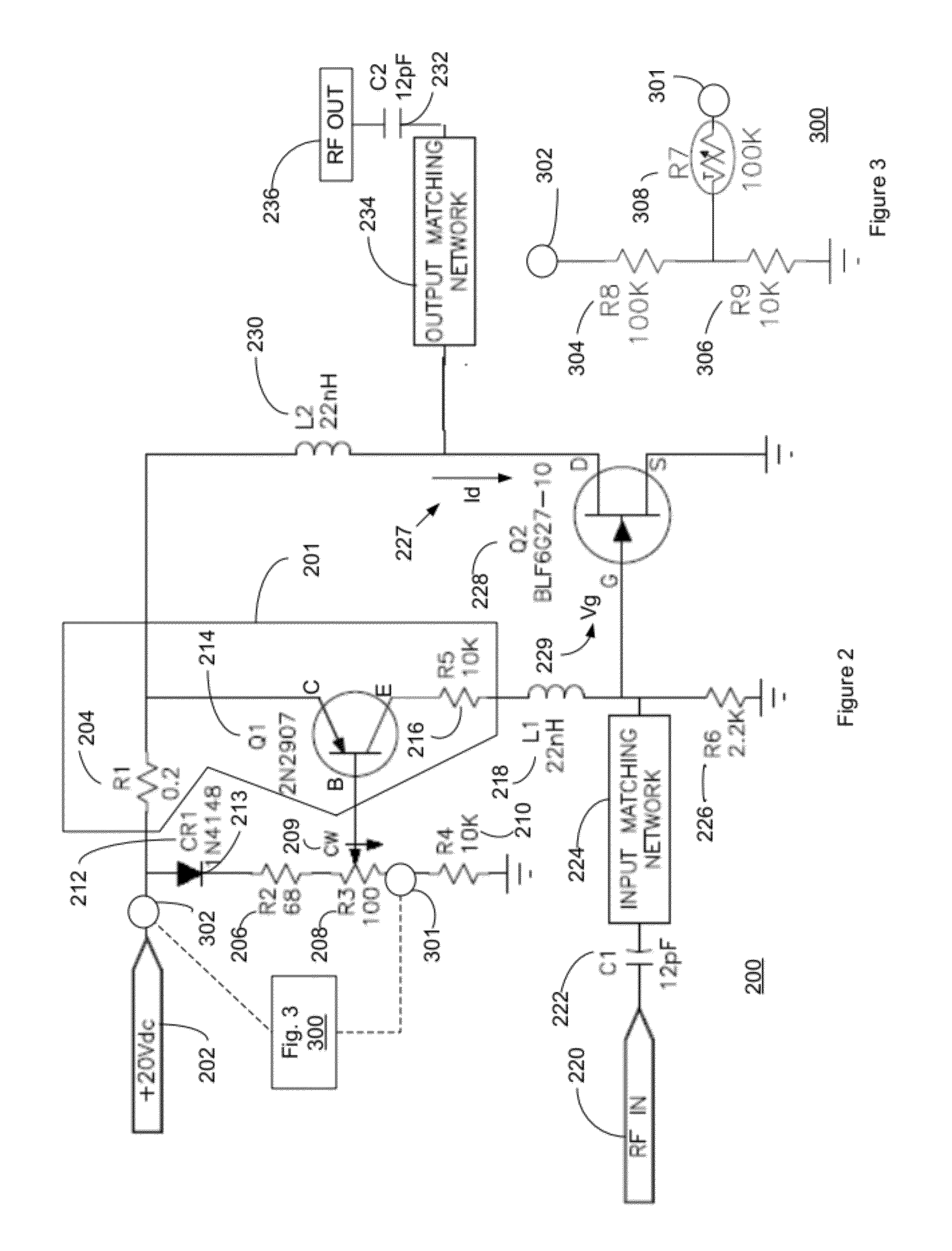
[0053]The present invention will now be described in more detail with reference to exemplary embodiments as shown in the accompanying drawings. While the present invention is described herein with reference to the exemplary embodiments, it should be understood that the present invention is not limited to such exemplary embodiments. Those possessing ordinary skill in the art and having access to the teachings herein will recognize additional implementations, modifications, and embodiments, as well as other applications for use of the invention, which are fully contemplated herein as within the scope of the present invention as disclosed and claimed herein, and with respect to which the present invention could be of significant utility.

[0054]The following exemplary circuits contain values which are typical for operation at +20VDC and in the 2 to 3 GHz band and help explain the inventive contribution in terms of performance. Although the invention may be described in examples in the GH...


PUM


Abstract

A feedback gate bias circuit for use in radio frequency amplifiers to more effectively control operation of LDFET, GaNFET, GaAsFET, and JFET type transistors used in such circuits. A transistor gate bias circuit that senses drain current and automatically adjusts or biases the gate voltage to maintain drain current independently of temperature, time, input drive, frequency, as well as from device to device variations. Additional circuits to provide temperature compensation, RF power monitoring and drain current control, RF output power leveler, high power gain block, and optional digital control of various functions. A gate bias circuit including a bias sequencer and negative voltage deriver for operation of N-channel depletion mode devices.

Description

CROSS-REFERENCE TO RELATED PATENT APPLICATIONS[0001]This patent application claims priority to U.S. Provisional Patent Application No. 61 / 340,960, filed Mar. 25, 2010, entitled “METHOD AND SYSTEM FOR PROVIDING AUTOMATIC GATE BIAS FOR FIELD EFFECT TRANSISTORS,” and to U.S. patent application Ser. No. 13 / 072,474, filed Mar. 25, 2011, entitled “METHOD AND SYSTEM FOR PROVIDING AUTOMATIC GATE BIAS FOR FIELD EFFECT TRANSISTORS,” which application is to issue May 29, 2012 as U.S. Pat. No. 8,188,794, all of which are hereby incorporated by reference herein in their entirety.FIELD OF THE INVENTION[0002]The present invention relates generally to apparatus and method for amplifying radio frequency (RF) signals, including microwave RF signals. More particularly, the present invention pertains to a transistor gate bias circuit for RF amplifier applications to overcome device variations and changing operating conditions to control and maintain transistor drain current.BACKGROUND OF THE INVENTION[...

Claims


Application Information

Patent Timeline
Patent Type & Authority Applications(United States)
IPC IPC(8): H03G3/30
CPCH03F1/301H03F3/16H03F3/19H03F2200/465H03F2200/15H03F2200/444H03F2200/462H03F1/0261
Inventor LAUTZENHISER, LLOYD
Owner EMHISER RES
Why Eureka
Try Eureka