Circuit board, electronic apparatus, and noise blocking method

Inactive Publication Date: 2012-12-27
NEC CORP
View PDF19 Cites 16 Cited by
  • Summary
  • Abstract
  • Description
  • Claims
  • Application Information

AI Technical Summary

Benefits of technology

[0009]The invention is made in consideration of the above-mentioned circumstances and an object thereof is to provide a circuit board, an electronic apparatus, and a noise blocking method, which include plural separated conductors and can prevent leakage of noise radiated from the gaps between the conductors.
[0013]According to the aspects of the invention, it is possible to provide a circuit board, an electronic apparatus, and a noise blocking method, which include plural separated conductors and can prevent leakage of noise radiated from the gaps between the conductors.

Problems solved by technology

Accordingly, even when an EBG structure is constituted in the conductive layer, a satisfactory noise countermeasure is not achieved.

Method used


Image

  • Circuit board, electronic apparatus, and noise blocking method
  • Circuit board, electronic apparatus, and noise blocking method
  • Circuit board, electronic apparatus, and noise blocking method

Examples


first embodiment

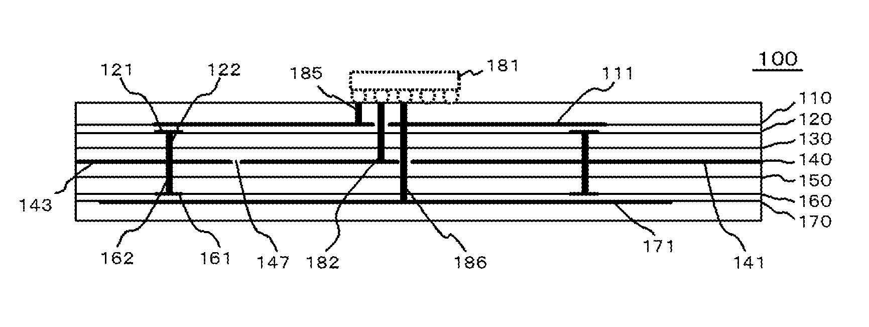
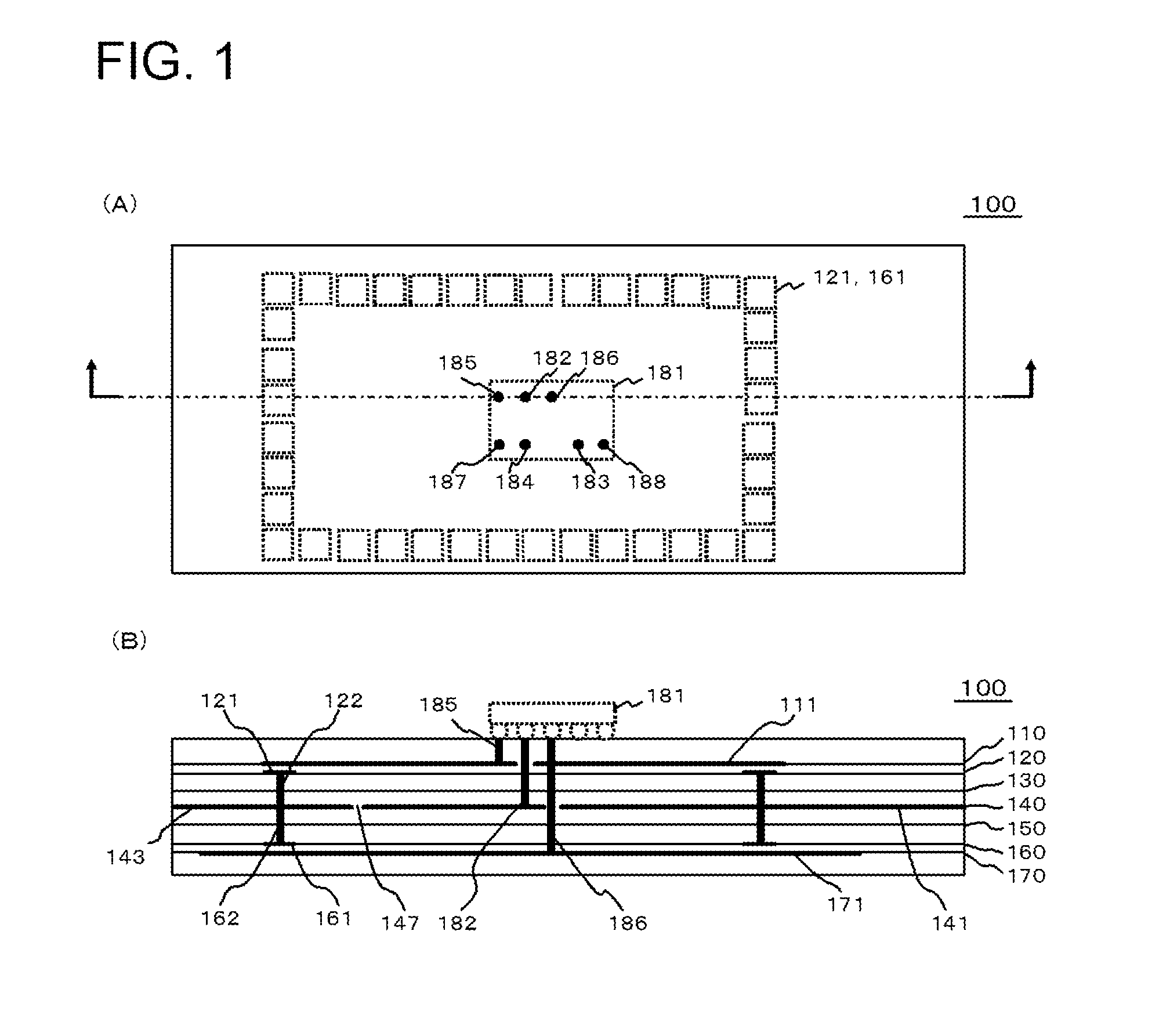
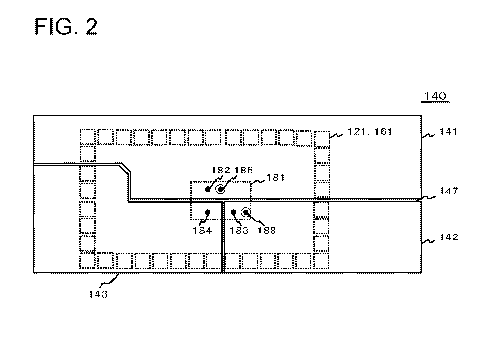
[0043]FIG. 1 shows a plan view and a cross-sectional view of a circuit board 100 according to a first embodiment of the invention. More specifically, FIG. 1(A) is a plan view of the circuit board 100 and FIG. 1(B) is a cross-sectional view of the circuit board 100 taken along the indicated sectional line in FIG. 1(A). The circuit board 100 is a multi-layered board including at least an A layer 110, a B layer 120, a C layer 130, a D layer 140, an E layer 150, an F layer 160, and a G layer 170 which are opposing each other. The circuit board 100 may include a layer other than the seven layers. For example, a dielectric layer may be located between the layers. The circuit board 100 may further include holes or vias not shown in the drawing without conflicting with the configuration of the invention. Signal lines may be arranged in the seven layers without conflicting with the configuration of the invention.

[0044]In FIG. 1, an electronic device 181 is indicated by a dotted line. This me...

second embodiment

[0121]FIG. 14 shows a plan view and a cross-sectional view of a circuit board 200 according to a second embodiment of the invention. More specifically, FIG. 14(A) is a plan view of the circuit board 200 and FIG. 14(B) is a cross-sectional view of the circuit board 200 taken along the indicated sectional line in FIG. 14(A). The circuit board 200 is a multi-layered board including at least an A layer 210, a B layer 220, a C layer 230, a D layer 240, an E layer 250, an F layer 260, and a G layer 270 which are opposing each other. The circuit board 200 may include a layer other than the seven layers. For example, a dielectric layer may be located between the layers. The circuit board 200 may further include holes or vias not shown in the drawing without conflicting with the configuration of the invention. Signal lines may be arranged in the seven layers without conflicting with the configuration of the invention.

[0122]An electronic device 281 is mounted on the surface of the circuit boa...

third embodiment

[0159]FIG. 22 shows a plan view and a cross-sectional view of a circuit board 300 according to a third embodiment of the invention. More specifically, FIG. 22(A) is a plan view of the circuit board 300 and FIG. 22(B) is a cross-sectional view of the circuit board 300 taken along the indicated sectional line in FIG. 22(A). The circuit board 300 is a multi-layered board including at least an A layer 310, a B layer 320, a C layer 330, a D layer 340, an E layer 350, an F layer 360, a G layer 370, and an H layer 380 which are opposing each other. The circuit board 300 may include a layer other than the eight layers. The circuit board 300 may further include holes or vias not shown in the drawing without conflicting with the configuration of the invention. Signal lines may be arranged in the eight layers without conflicting with the configuration of the invention.

[0160]Plural penetration vias 382 are repeatedly arranged in the circuit board 300. The penetration via 382 is formed by formin...


PUM


Abstract

A circuit board (100) includes power supply planes (141, 143) arranged with gaps (147) in a D layer (140), connection members (182, 183, 184) electrically connecting at least one of the power supply planes (141, 143) to an electronic device (181), plural conductor elements (121) repeatedly arranged to surround at least some of the gaps (147) and the connection members (182, 183, 184), and ground planes (111, 171) being located in an A layer (110) or a G layer (170) and extending in a second region or a third region including a region opposing the first region and a region opposing the conductor elements (121).

Description

TECHNICAL FIELD[0001]The present invention relates to a circuit board, an electronic apparatus, and a noise blocking method.BACKGROUND ART[0002]In electronic apparatuses, noise generated from an electronic device propagates in a parallel plate including a power supply plane and a ground plane as a kind of waveguide and may adversely affect other electronic devices or nearby radio circuits. Accordingly, in such an electronic apparatus, noise countermeasures are generally taken and various techniques have been developed.[0003]In recent years, it has been known that propagation characteristics of electromagnetic waves can be controlled by periodically arranging a conductor pattern having a specific structure (hereinafter, referred to as a metamaterial). Particularly, a metamaterial constructed to suppress propagation of electromagnetic waves in a specific frequency band is referred to as an electromagnetic bandgap structure (hereinafter, referred to as an EBG structure). A noise counte...

Claims


Application Information

Patent Timeline
IPC IPC(8): H05K1/16
CPCH05K1/0236H05K1/0243H05K1/0298H05K1/116H05K1/162H05K1/165H05K2201/09618H05K2201/09663H05K2201/0969H05K2201/0979H05K2201/10371H05K2201/10674H05K1/024H01L2224/16225H01L2924/15174H01L2924/16152
Inventor TOYAO, HIROSHIKUSUMOTO, MANABUKOBAYASHI, NAOKIANDO, NORIAKI
Owner NEC CORP
Why Eureka
Try Eureka