

Organic Light-Emitting Diode
- Summary
- Abstract
- Description
- Claims
- Application Information
AI Technical Summary
Benefits of technology
Problems solved by technology
Method used
Image

Examples
example 1
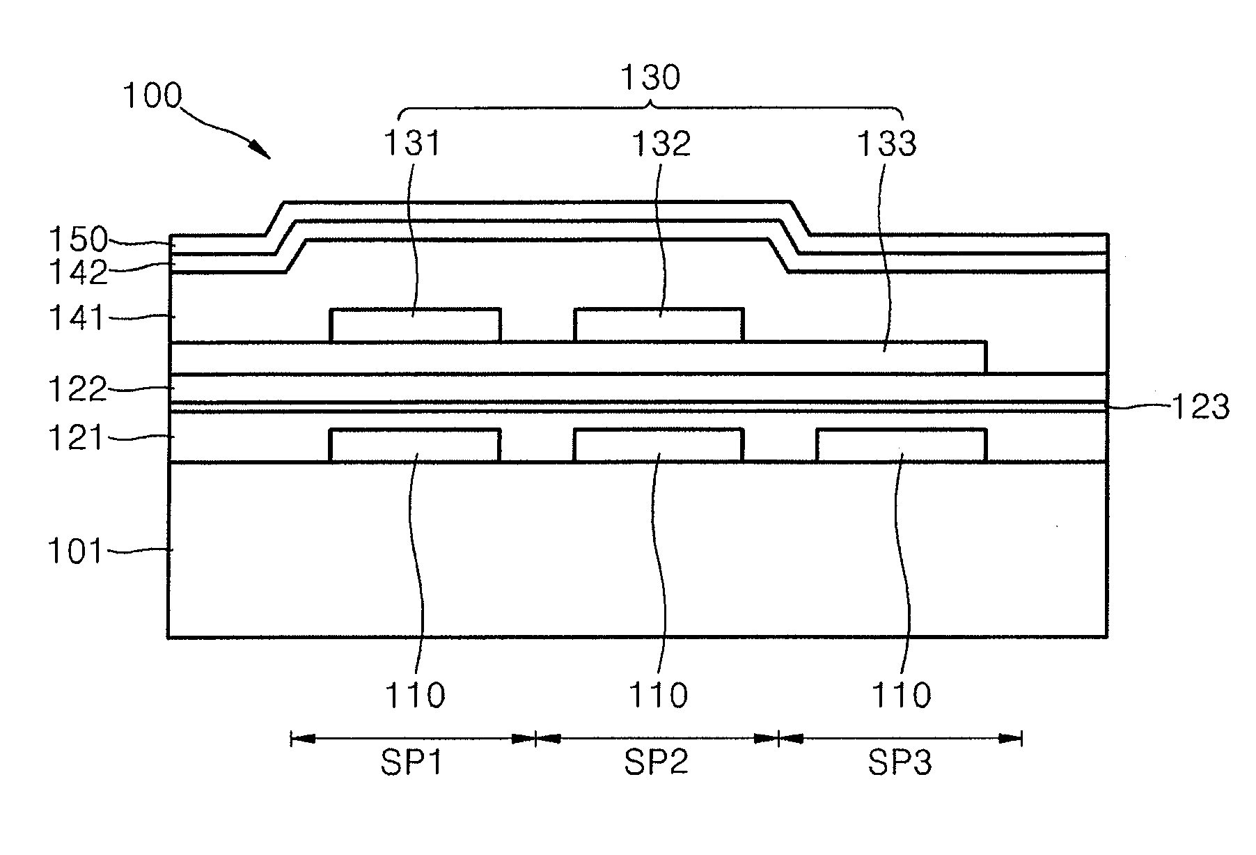
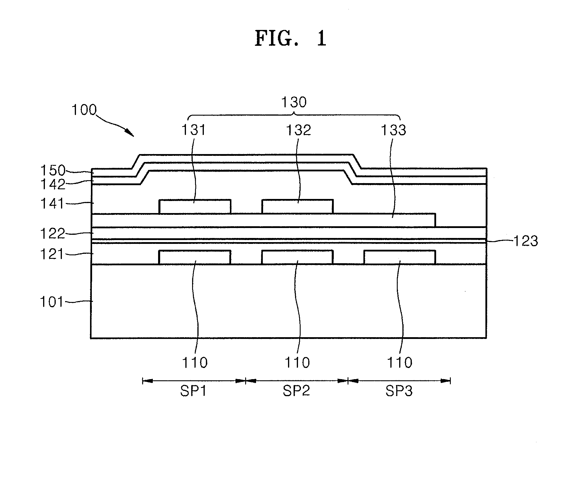
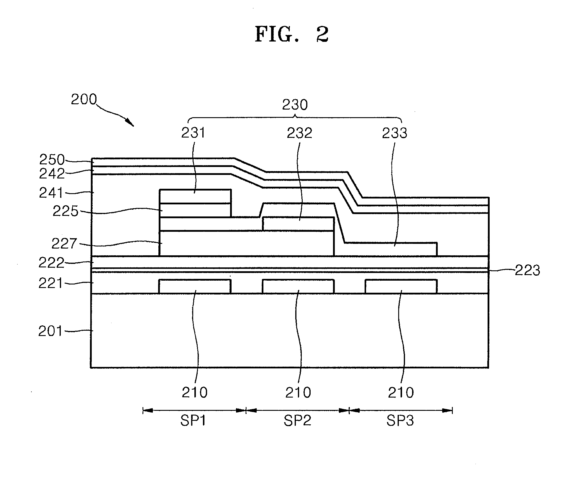
[0116]As an anode, 15 Ω / cm2 (1200 Å) of an ITO glass substrate from Corning Co., Ltd. was cut to a size of 50 mm×50 mm×0.7 mm, and ultrasonically washed with isopropyl alcohol and pure water for 5 minutes each. Subsequently, UV rays were irradiated to the resulting ITO glass substrate for 30 minutes, and the ITO glass substrate was washed with ozone and mounted on a vacuum deposition device. 2-TNATA was vacuum deposited on the ITO glass substrate to form a hole injection layer having a thickness of 650 Å, hexa-azatriphenylene hexacarbonitrile (HAT-CN) was vacuum deposited on the hole injection layer to form an intermediate layer having a thickness of 50 Å, and 4,4′-bis[N-(1-naphthyl)-N-phenylamino]biphenyl (NPB) was vacuum deposited on the intermediate layer to form a hole transport layer having a thickness of 700 Å. Compound 105 was vacuum deposited on the hole transport layer over a first sub-pixel and a second sub-pixel to form a second optical thickness auxiliary layer having a ...
PUM
 Abstract
Description
Claims
Application Information