High-voltage integrated circuit device

a high-voltage integrated circuit and integrated circuit technology, applied in semiconductor devices, semiconductor/solid-state device details, electrical devices, etc., can solve problems such as increasing the number of invalid regions, and achieve the effect of preventing an erroneous operation or the destruction of logic parts

Active Publication Date: 2013-01-03
FUJI ELECTRIC CO LTD
View PDF6 Cites 15 Cited by
  • Summary
  • Abstract
  • Description
  • Claims
  • Application Information

AI Technical Summary

Benefits of technology

[0059]According to the invention described above, the electron hole injection that is caused when a negative-voltage surge is input can be locally diminished by providing the section of the high-voltage junction terminating region, whose distance to the intermediate-potential region is shorte

Problems solved by technology

However, providing a distance of at least 100 μm between a contact region and an intermediate-potential region in all regions

Method used


Image

  • High-voltage integrated circuit device
  • High-voltage integrated circuit device
  • High-voltage integrated circuit device

Examples


embodiment 1

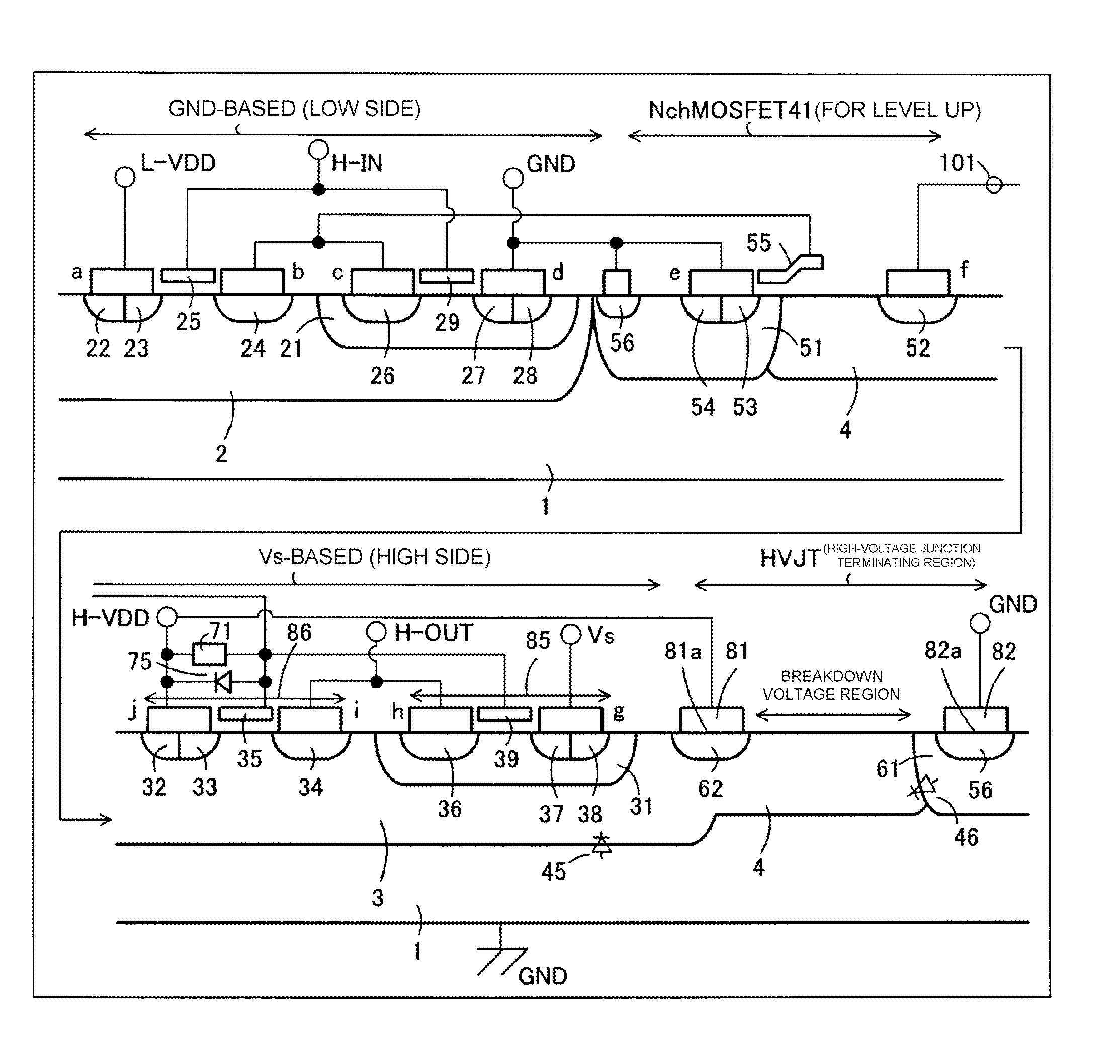
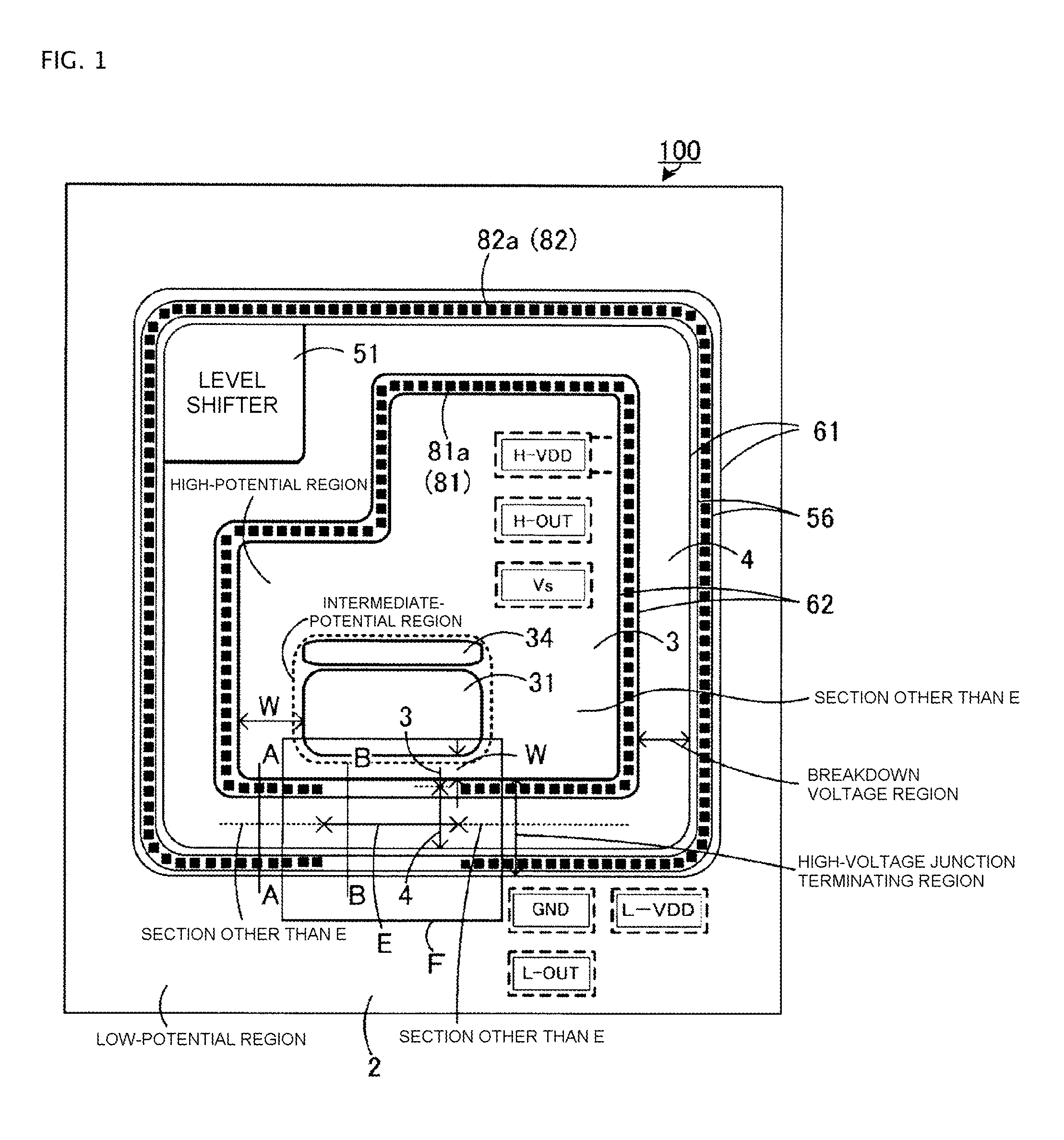
[0079]FIG. 1 is a plan view showing substantial parts of a high-voltage integrated circuit device 100 according to Embodiment 1 of the present invention. FIG. 2 is a cross-sectional diagram showing the entire substantial parts, taken along a section line A-A of FIG. 1 in a parallel direction. In FIGS. 1 and 2 the same reference numerals are used for explaining the configurations corresponding to the configurations shown in FIGS. 9 to 13.

[0080]FIG. 3 is a substantial plan view showing flows of an electron hole and an electron by using an enlarged view of an F part shown in FIG. 1. Note that a region shown in diagonal dashed lines represents a section (opposition section) E in which a part of an intermediate-potential region is disposed in proximity to an n-contact region 62. This section E is a section of a high-voltage junction terminating region, whose distance W to the intermediate-potential region is shorter than those of other sections.

[0081]FIG. 4 is a substantial cross-section...

second embodiment 2

[0113]FIG. 5 is a plan view showing substantial parts of a high-voltage integrated circuit device 200 according to Embodiment 2 of the present invention. FIG. 6 is a cross-sectional diagram showing the substantial parts of the high-voltage integrated circuit device 200 according to Embodiment 2 of the present invention. FIG. 6(a) is a substantial cross-sectional diagram showing a cross-sectional structure taken along a section line A-A shown in FIG. 5. FIG. 6(b) is a substantial cross-sectional diagram showing a cross-sectional structure taken along a section line B-B shown in FIG. 5.

[0114]The difference between the high-voltage integrated circuit device 200 shown in FIG. 5 and the high-voltage integrated circuit device 100 shown in FIG. 1 is that the high-voltage integrated circuit device 200 has a double RESURF structure 87 formed in the opposition section E of the high-voltage junction terminating region, whose distance W to the intermediate-potential region is short, without rem...

embodiment 3

[0122]FIG. 7 is a plan view showing substantial parts of a high-voltage integrated circuit device 300 according to Embodiment 3 of the present invention. FIG. 8 is a cross-sectional diagram showing the substantial parts of the high-voltage integrated circuit device 300 according to Embodiment 3 of the present invention. FIG. 8(a) is a substantial cross-sectional diagram showing a cross-sectional structure taken along a section line A-A shown in FIG. 7. FIG. 8(b) is a substantial cross-sectional diagram showing a cross-sectional structure taken along a section line C-C shown in FIG. 7.

[0123]The high-voltage integrated circuit device 300 shown in FIG. 7 is different from the high-voltage integrated circuit device 200 shown in FIG. 5 in that, in the opposition section E whose distance W to the Vs potential region is short, the n-well region 4, which the high-voltage junction terminating region, is made wide compared to the other sections, instead of forming the p-top layer 63 thereon. ...


PUM


Abstract

A high-voltage integrated circuit device has formed therein a high-voltage junction terminating region that is configured by a breakdown voltage region formed of an n-well region, a ground potential region formed of a p-region, a first contact region and a second contact region. An opposition section of the high-voltage junction terminating region, whose distance to an intermediate-potential region formed of a p-drain region is shorter than those of other sections, is provided with a resistance higher than those of the other sections. Accordingly, a cathode resistance of a parasitic diode formed of the p-region and the n-well region increases, locally reducing the amount of electron holes injected at the time of the input of a negative-voltage surge. As a result, an erroneous operation or destruction of a logic part of a high-side circuit can be prevented when the negative-voltage surge is applied to an H-VDD terminal or a Vs terminal.

Description

TECHNICAL FIELD[0001]The present invention relates to a high-voltage integrated circuit device (HVIC) that is used, for example, in transmitting an on / off drive signal to a gate of a switching power device of a PWM inverter, a switching power supply, and the like. The present invention particularly relates to a high-voltage integrated circuit device capable of preventing the occurrence of an erroneous operation caused due to an overcurrent that flows when a negative-voltage surge is input to the circuit.BACKGROUND ART[0002]An HVIC of an element separation type that utilizes high-voltage junction is used as means for driving a switching power device that configures an upper arm of a power reverse conversion (AC-DC conversion) bridge circuit of a PWM inverter or the like. The HVIC can accomplish high functionality by detecting an overcurrent when the switching power device malfunctions and having temperature detecting means, and can achieve reductions of the size of a power supply sys...

Claims


Application Information

Patent Timeline
IPC IPC(8): H01L23/48
CPCH01L21/823481H01L21/823493H01L27/0203H01L27/088H01L2924/0002H01L2924/00
Inventor YAMAJI, MASAHARU
Owner FUJI ELECTRIC CO LTD
Why Eureka
Try Eureka