
Method of forming polysilicon resistor during replacement metal gate process and semiconductor device having same

a technology of metal gate replacement and polysilicon, which is applied in the direction of semiconductor devices, diodes, electrical devices, etc., can solve the problem of not using the high resistive properties of polysilicon

Active Publication Date: 2013-01-17
SAMSUNG ELECTRONICS CO LTD
View PDF6 Cites 18 Cited by
  • Summary
  • Abstract
  • Description
  • Claims
  • Application Information

AI Technical Summary

Benefits of technology

The patent describes a method for manufacturing a semiconductor device by forming a first gate stack portion on a substrate, depositing a second gate stack portion on the substrate, and forming a resistor portion in a recessed portion of the substrate. The method also includes removing the first and second polysilicon layers from the first and second gate stack portions and depositing a high-K dielectric material on the exposed portions of the substrate. The method further includes performing a chemical mechanical polishing to planarize the top surface of the semiconductor device. The patent also describes a semiconductor device and a computer system that includes the semiconductor device. The technical effects of the patent include improving the manufacturing process for semiconductor devices and improving the performance of the semiconductor devices.

Problems solved by technology

As a result, the high resistive properties of polysilicon are not utilized for resistors on a substrate in which RMG processing has been performed.

Method used


Image

  • Method of forming polysilicon resistor during replacement metal gate process and semiconductor device having same
  • Method of forming polysilicon resistor during replacement metal gate process and semiconductor device having same
  • Method of forming polysilicon resistor during replacement metal gate process and semiconductor device having same

Examples


Embodiment Construction

[0032]Exemplary embodiments of the present inventive concept now will be described more fully hereinafter with reference to the accompanying drawings. This inventive concept may, however, be embodied in many different forms and should not be construed as limited to the embodiments set forth herein.

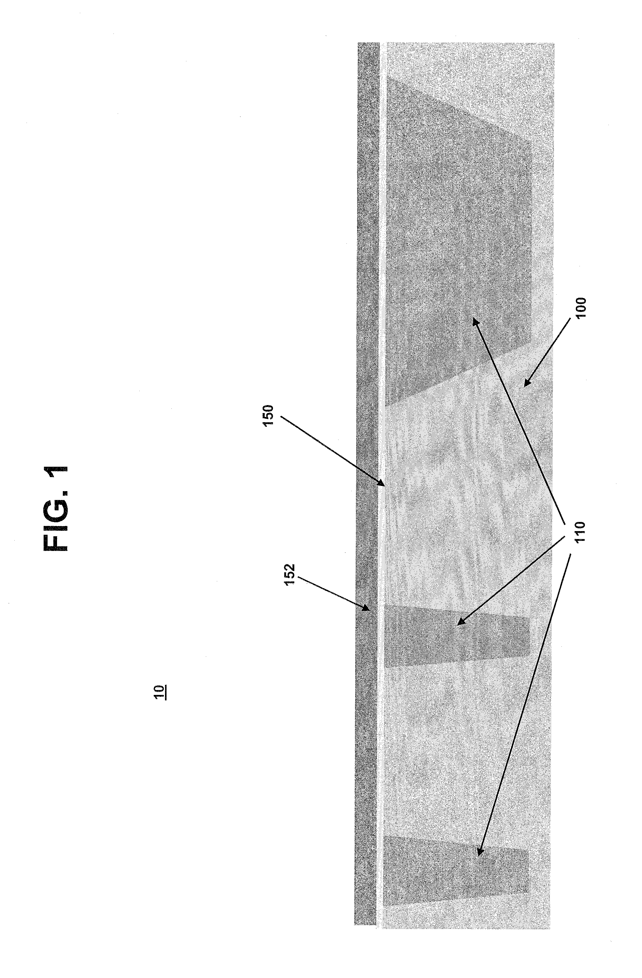
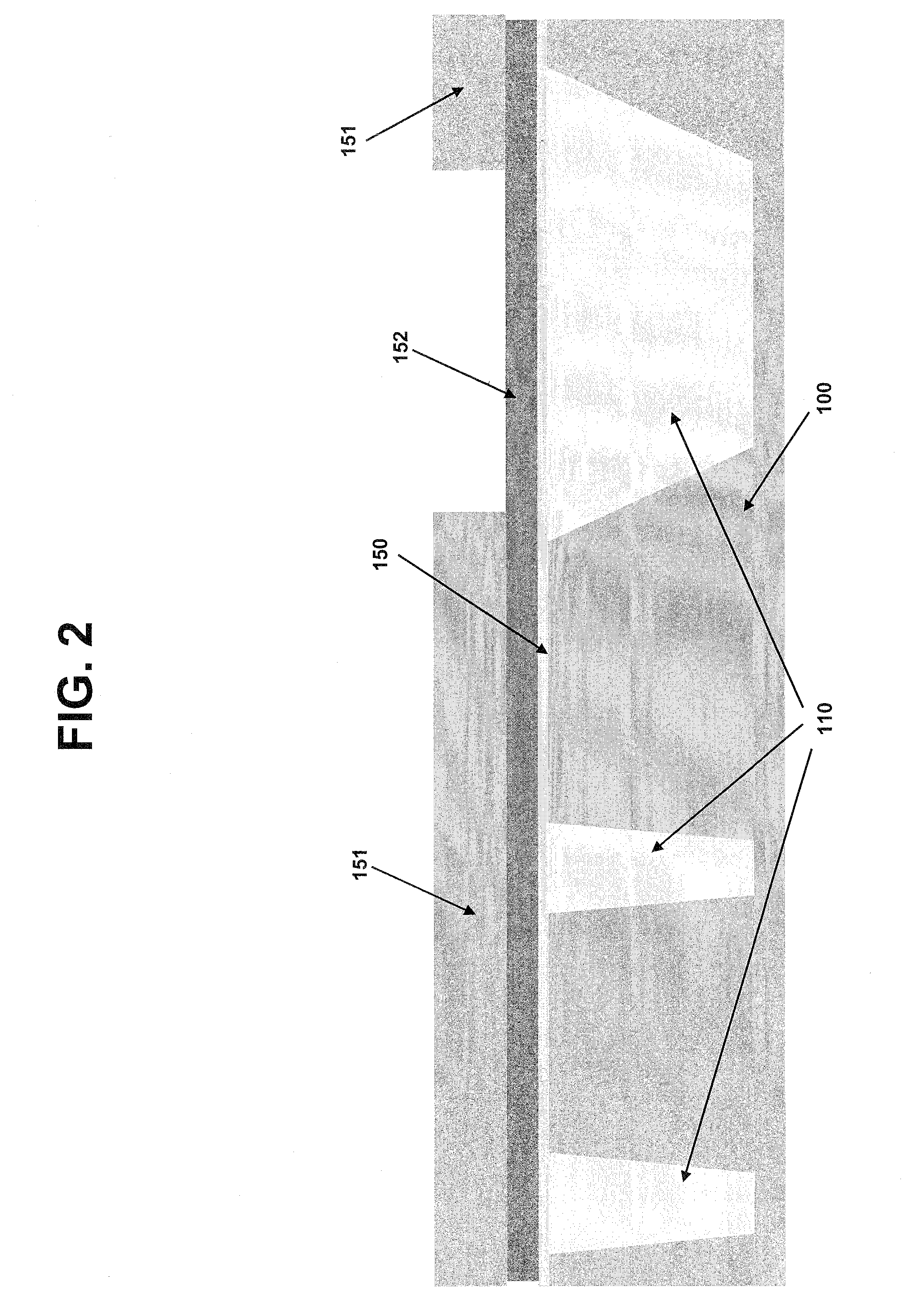
[0033]Referring to FIG. 1, according to an embodiment of the present inventive concept, a semiconductor device 10 includes a substrate 100 including a plurality of shallow trench isolation (STI) regions 110. On the substrate, a first single gate (SG) field-effect transistor (FET) will be formed between first and second STI regions 110 (looking from left to right in FIG. 1), a second SG FET will be formed between second a third STI regions 110, and a resistor structure will be formed over the third STI region 110. As shown in FIG. 1 a gate oxide layer 150 is deposited on the substrate 100 and a polysilicon layer 152 is formed on the gate oxide layer 150. According to an embodiment, the poly...


PUM


Abstract

A method for manufacturing a semiconductor device, comprising forming a first gate stack portion on a surface of a substrate, the first gate stack portion including a first gate oxide layer and a first polysilicon layer on the first gate oxide layer, forming a second gate stack portion on the surface of the substrate, the second gate stack portion including a second gate oxide layer and a second polysilicon layer on the second gate oxide layer, forming a resistor portion in a recessed portion of the substrate below the surface of the substrate, the resistor portion including a third polysilicon layer, and removing the first and second polysilicon layers from the first and second gate stack portions to expose the first and second gate oxide layers, wherein at least one of a dielectric layer and a stress liner cover a top surface of the resistor portion during removal of the first and second polysilicon layers.

Description

BACKGROUND[0001]1. Technical Field[0002]The present disclosure relates to method of forming a polysilicon resistor during a replacement metal gate process, and a semiconductor device having the polysilicon resistor.[0003]2. Discussion of the Related Art[0004]Metal-oxide-semiconductor (MOS) transistors using polysilicon gate electrodes are known. Polysilicon material is able to tolerate high temperature processing better than most metals, so that polysilicon can be annealed at high temperatures along with source and drain regions. In addition, polysilicon blocks ion implantation of doped atoms into a channel region, facilitating the formation of self-aligned source and drain structures after gate patterning is completed.[0005]The high resistivities of polysilicon materials, as compared to most metal materials result in polysilicon gate electrodes that operate at much slower speeds than gates made of metallic materials. One way of compensating for the higher resistance of polysilicon ...

Claims


Application Information

Patent Timeline
IPC IPC(8): H01L21/20H01L27/06B82Y40/00
CPCH01L21/28123H01L29/4966H01L29/7833H01L29/7843H01L29/165H01L28/20H01L21/823481H01L21/823842H01L21/823878H01L27/0629H01L21/82345H01L29/66545
Inventor KIM, JU YOUNKIM, JEDON
Owner SAMSUNG ELECTRONICS CO LTD
Features
  • Generate Ideas
  • Intellectual Property
  • Life Sciences
  • Materials
  • Tech Scout
  • Unparalleled Data Quality
  • Higher Quality Content
  • 60% Fewer Hallucinations
Learn More