Negative Ion Control for Dielectric Etch

a dielectric etch and negative ion technology, applied in the field of negative ion control of dielectric etch, can solve the problem that the rf power supply is not an efficient way of etching

Active Publication Date: 2013-01-24
LAM RES CORP
View PDF24 Cites 23 Cited by
  • Summary
  • Abstract
  • Description
  • Claims
  • Application Information

AI Technical Summary

Benefits of technology

[0008]Embodiments of the present invention provide methods, systems, and computer programs for negative ion control in a capacitively-co...

Problems solved by technology

However, pulsing the RF power supply is not an efficient way of et...

Method used


Image

  • Negative Ion Control for Dielectric Etch
  • Negative Ion Control for Dielectric Etch
  • Negative Ion Control for Dielectric Etch

Examples


Embodiment Construction

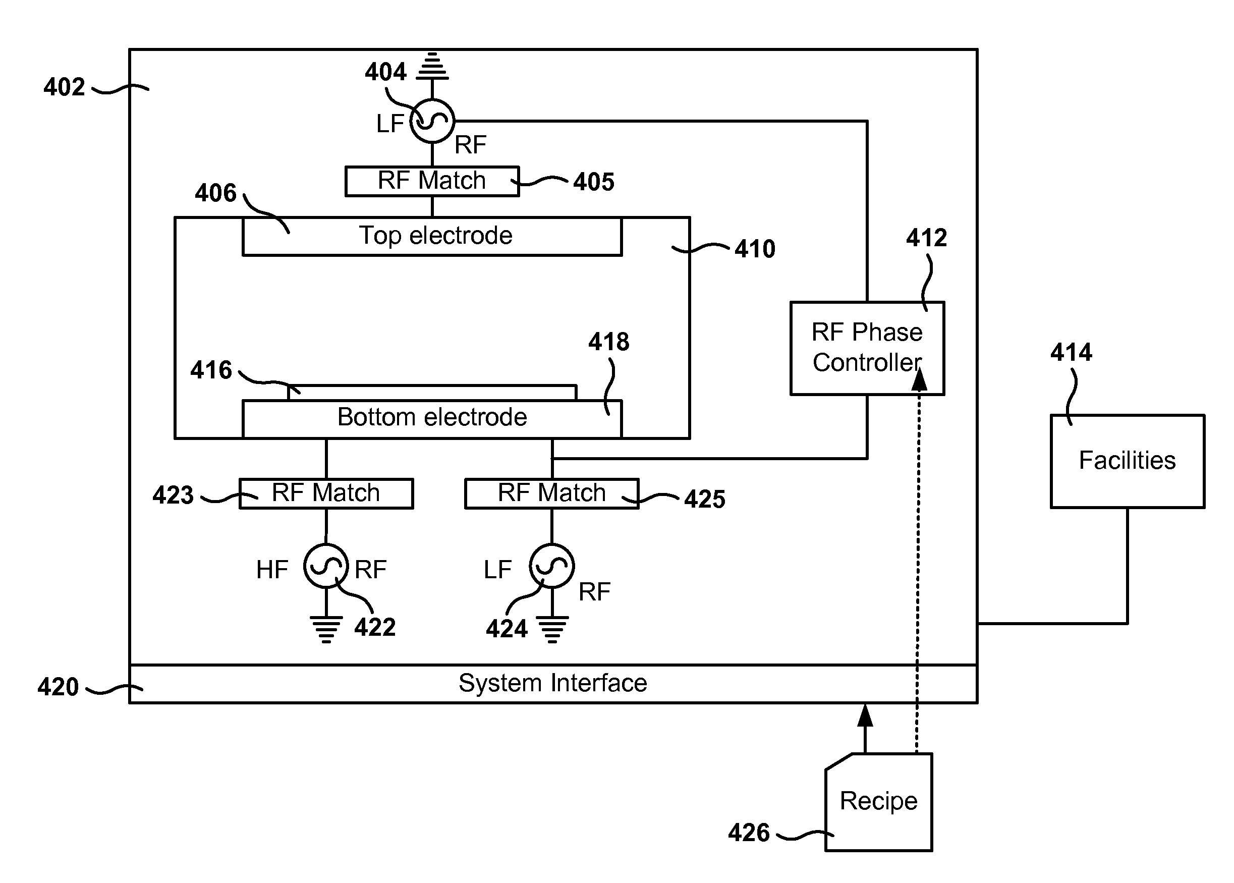
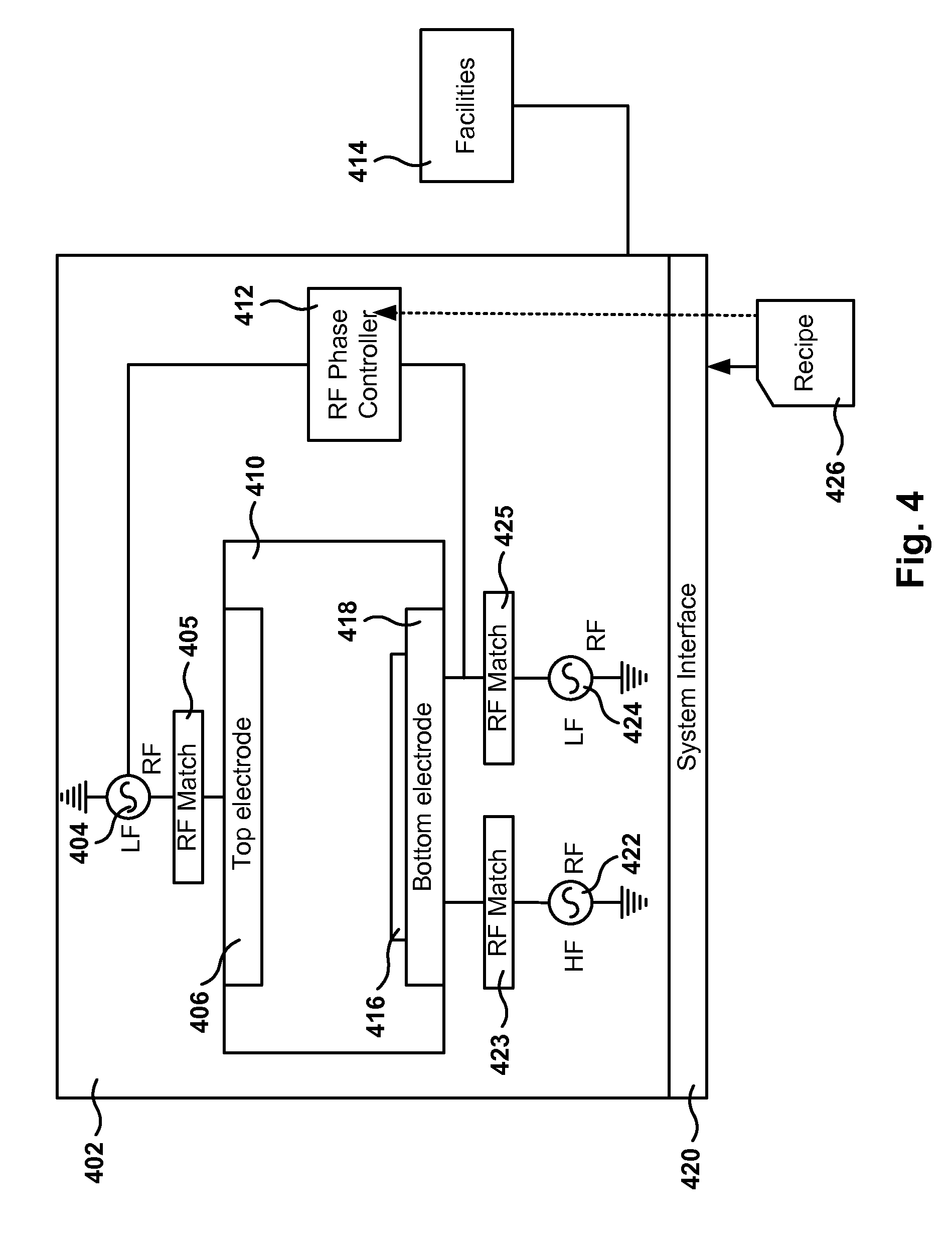
[0025]Embodiments of the invention perform substrate etching utilizing negative ions. The top electrode is powered with a low frequency radio frequency (RF) whose is phase is controlled based on the phase of another low frequency RF applied to the bottom electrode. Negative ions born at the top sheath travel through the plasma bulk, and approach the wafer surface when the bottom sheath potential is approximately at a minimum.

[0026]It will be apparent, that the present embodiments may be practiced without some or all of these specific details. In other instances, well known process operations have not been described in detail in order not to unnecessarily obscure the present embodiments.

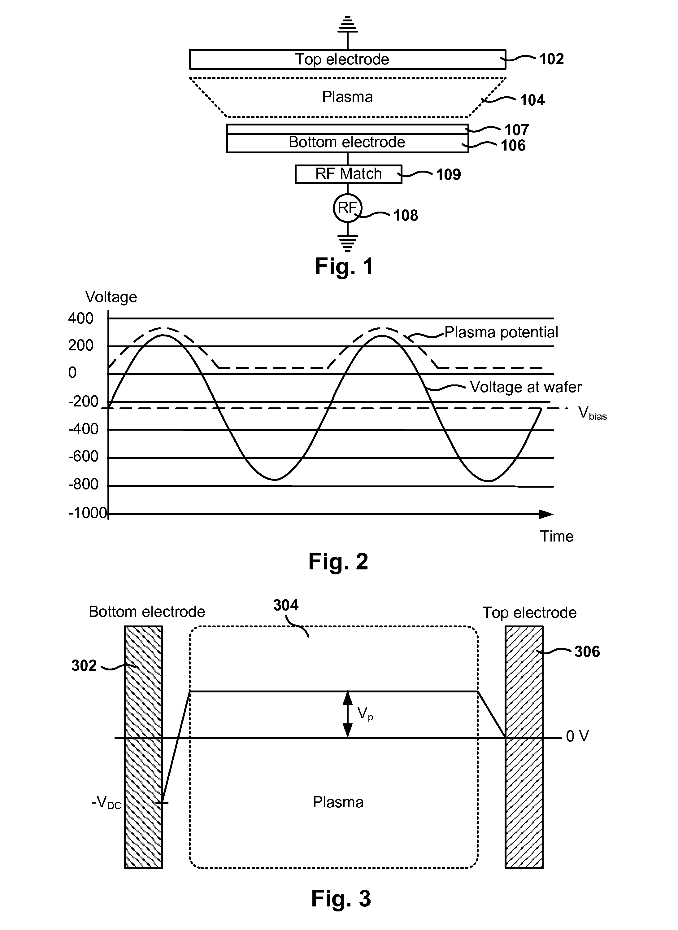
[0027]FIG. 1 shows an asymmetric etching chamber, according to one embodiment. Exciting an electric field between two electrodes is one of the methods to obtain RF gas discharge in an etching chamber. When an oscillating voltage is applied between the electrodes, the discharge obtained is referred to ...


PUM

PropertyMeasurementUnit
Distanceaaaaaaaaaa
Distanceaaaaaaaaaa
Frequencyaaaaaaaaaa

Abstract

Apparatus, methods, and computer programs for semiconductor processing in a capacitively-coupled plasma chamber are provided. A chamber includes a bottom radio frequency (RF) signal generator, a top RF signal generator, and an RF phase controller. The bottom RF signal generator is coupled to the bottom electrode in the chamber, and the top RF signal generator is coupled to the top electrode. Further, the bottom RF signal is set at a first phase, and the top RF signal is set at a second phase. The RF phase controller is operable to receive the bottom RF signal and operable to set the value of the second phase. Additionally, the RF phase controller is operable to track the first phase and the second phase to maintain a time difference between the maximum of the top RF signal and the minimum of the bottom RF signal at approximately a predetermined constant value, resulting in an increase of the negative ion flux to the surface of the wafer.

Description

BACKGROUND[0001]1. Field of the Invention[0002]The present invention relates to methods, systems, and computer programs for facilitating dielectric etching of a semiconductor device, and more particularly, methods, systems, and computer programs for facilitating negative ion control in a capacitively-coupled plasma (CCP) chamber.[0003]2. Description of the Related Art[0004]The manufacturing of integrated circuits includes immersing silicon substrates (wafers) containing regions of doped silicon into chemically-reactive plasmas, where the submicron device features (e.g., transistors, capacitors, etc.) are etched onto the surface. Once the first layer is manufactured, several back-end insulating (dielectric) layers are built on top of the first layer, where holes (also referred to as vias) and trenches are etched into the material for placement of the conducting interconnectors.[0005]SiO2 is a common dielectric used in semiconductor manufacturing. The plasmas used for SiO2 etching oft...

Claims


Application Information

Patent Timeline
IPC IPC(8): H01L21/66H01L21/3065
CPCH01J37/32091H01L21/31116H01J37/32137H01L21/67069H01J2237/3348H01J2237/334H01J2237/3343H01L21/3065C23C16/505C23C14/345H01L22/20H05H1/466
Inventor MARAKHTANOV, ALEXEIABATCHEV, MIRZAFER K.DHINDSA, RAJINDERHUDSON, ERICBAILEY, III, ANDREW D.
Owner LAM RES CORP
Why Eureka
Try Eureka