Sensor and sensor element

Active Publication Date: 2013-02-07
MICRO EPSILON MESSTECHNIK GMBH & CO KG
View PDF8 Cites 5 Cited by
  • Summary
  • Abstract
  • Description
  • Claims
  • Application Information

AI Technical Summary

Benefits of technology

The invention is a new type of sensor that has a unique design made up of multiple layers of ceramic. This design reduces the width of the sensor and increases the number of windings (which are loops of electrified material) per surface area. This offset winding arrangement also reduces the capacitive coupling between the windings, which improves the stability of the measurement signal. This new design helps to achieve better and more accurate readings from the sensor.

Problems solved by technology

Along with the aforesaid advantages of the ceramic coils there are however also technical limitations.
An increase of the inductance alone is however not expedient since with too high an inductance capacitive effects reduce the sensitivity of measurement or the time constant (and thus the temporal resolution) of the sensor will even become too high.
There the ratio between current-carrying layers and the insulating ceramic substrate is unfavorable.
Furthermore, the ceramic substrate is only available in certain thicknesses.
These two prerequisites make the embossing very time-consuming and expensive.
The therewith associated expulsion of material leads to different density distributions in the material which can create problems in further processing.
The process steps needed in addition, in comparison to the standard process, as well as tools and consumable materials, are elaborate and expensive.
Furthermore, at the edges of the photosensitive layer smearing can occur.
This is particularly critical for small structural sizes since thereby short circuits between the windings can occur.
The printing of an embossed layer proves to be difficult above all for relatively small line spacings and widths since the positioning of the paste over the embossing must be done precisely.
With imprecise positioning there arises at the edge of the winding smearing which after sintering can lead to short circuits.
Through the optimization of the coil design with the aid of embossing technology and with relatively high costs and great expenditure of time only limited improvements of the sensor characteristics can be achieved.
Laser processing is however relatively time-consuming.
This makes the process per se elaborate and expensive.
However, in so doing the faces of the cut are very rough.
The great roughness creates problems during later filling with paste.
Thus, for example, small air bubbles can arise which at the high sintering temperatures lead to stresses in the material due to the compressive expansion.
Furthermore, the roughness enlarges the surface of the conductive layer.
These effects have a negative effect on the electrical data of the sensor.

Method used


Image

  • Sensor and sensor element
  • Sensor and sensor element
  • Sensor and sensor element

Examples


Embodiment Construction

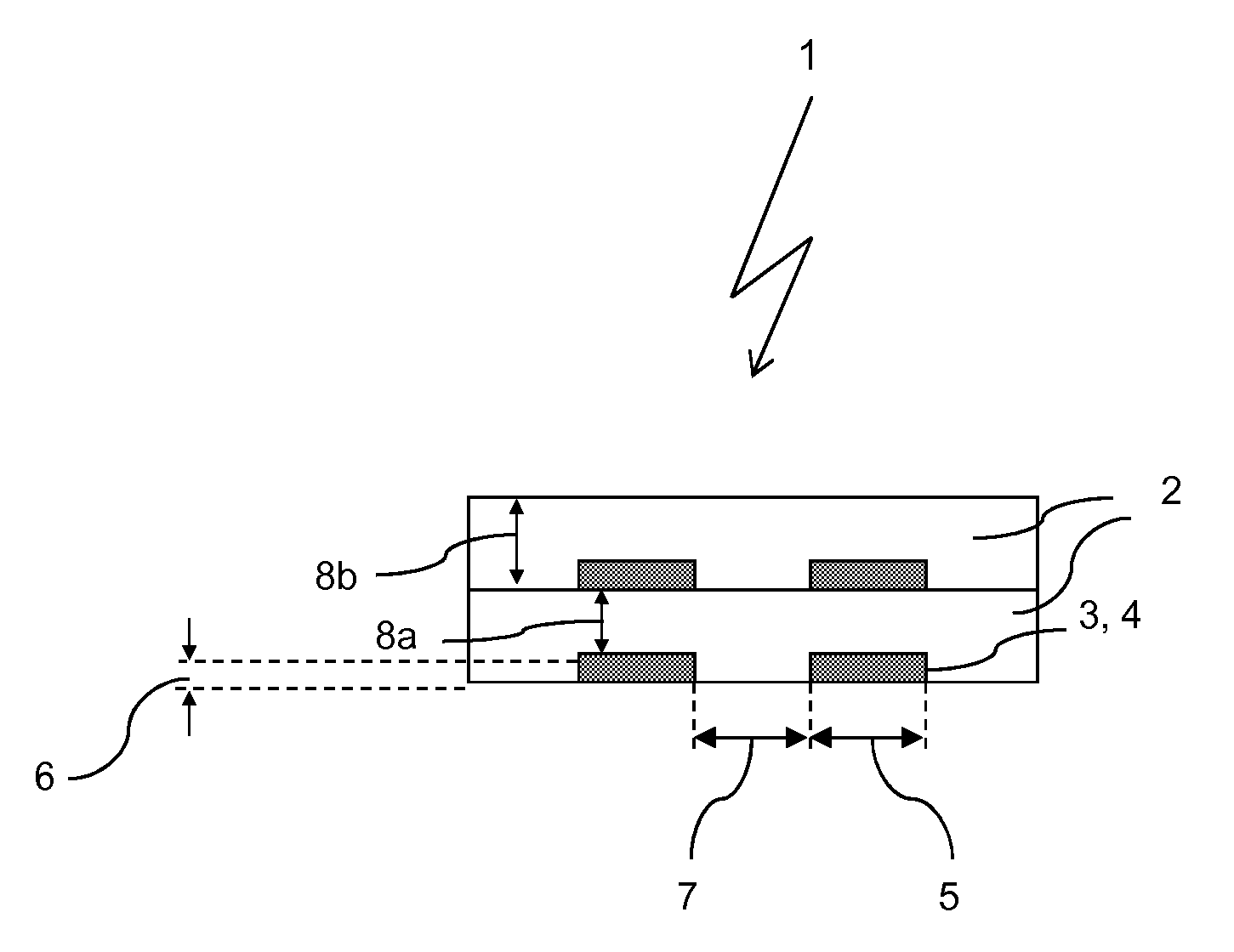
[0061]FIG. 1 shows in a schematic arrangement a standard coil 1 in cross section. In the embodiment example shown in FIG. 1 the coil comprises two layers 2 with windings 3 integrated there.

[0062]The winding 3 of the coil is defined by a line 4 which has a predefined line width 5 and a line thickness 6. The spacing between the lines 4 is denoted as the line spacing 7.

[0063]The spacing between the windings 3 of the layers 2 is denoted as the layer spacing 8a. Reference number 8b marks the thickness of an individual layer 2, and in the sequel will be denoted by 8b.

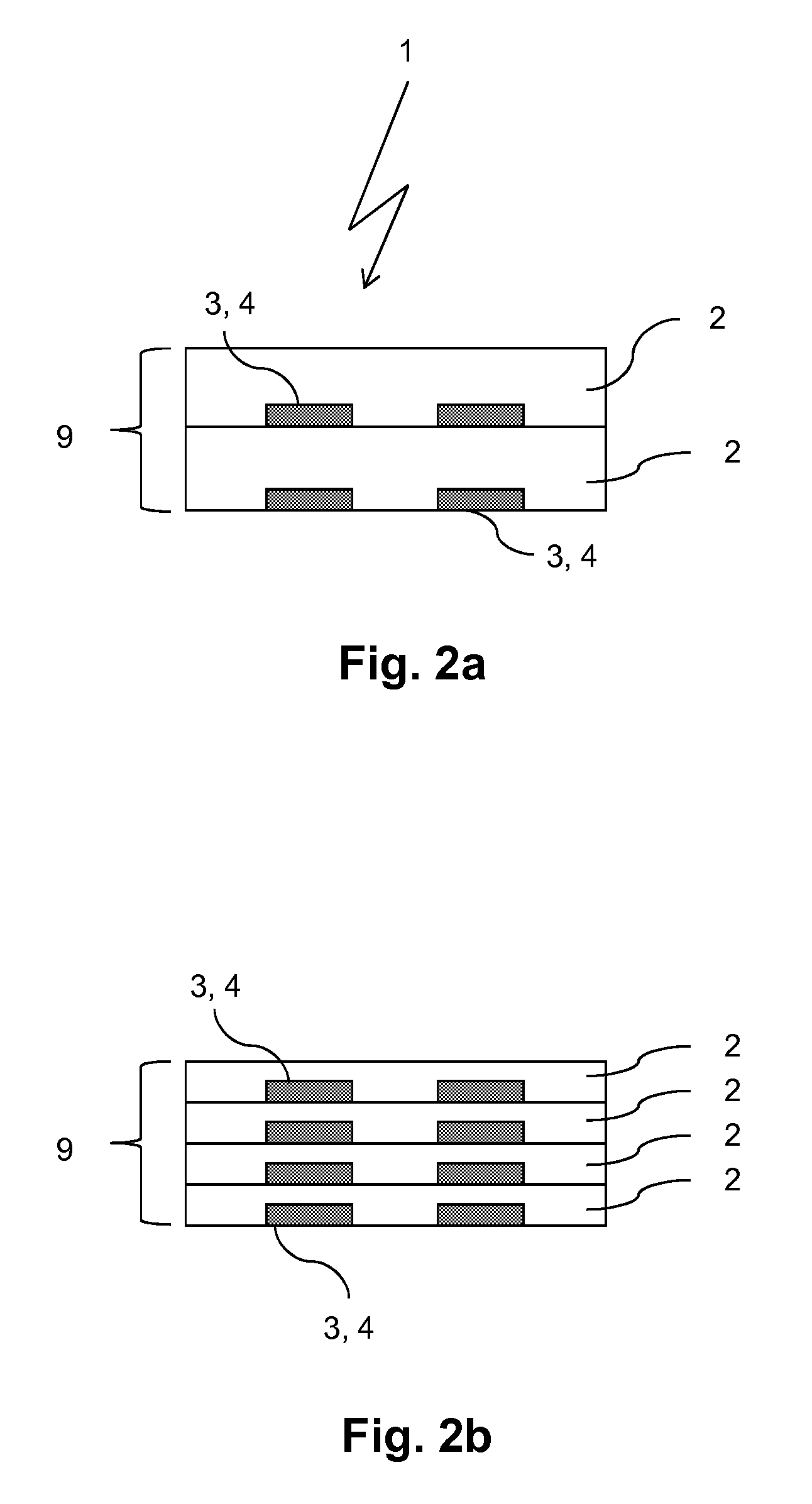
[0064]FIG. 2a shows once again the customary standard coil 1, from which the coil arrangement according to the invention and represented in FIG. 2b differs quite significantly, namely in that there in place of two layers 2 four layers 2 per unit of cross-sectional surface area 9 are provided. The four layers 2 provided according to FIG. 2b take up the same space as the two layers 2 in the customary standard coil 1 according ...


PUM


Abstract

Sensor with a one-layer or multi-layer sensor element operating in a contact-free manner and a housing comprising an electric / electronic connection and, in given cases, electronic components, where the sensor element comprises a coil arrangement whose windings have a defined line width, line thickness, and line spacing per layer and whose layers have a defined layer thickness and, in given cases, a defined layer spacing, characterized in that the sensor element is built up from ceramic layers in the sense of multi-layer ceramics and that with respect to traditional coil arrangements the line width is reduced and the number of windings per cross-sectional surface area is increased.

Description

CROSS REFERENCE TO RELATED APPLICATIONS[0001]This application claims priority to German Application No. 10 2011 109 553.9, filed Aug. 5, 2011, and is hereby incorporated by reference in its entirety.BACKGROUND[0002]1. Technical Field[0003]The invention concerns a sensor with a one-layer or multi-layer sensor element operating in a contact-free manner and a housing comprising an electric / electronic connection and, in given cases, electronic components, where the sensor element comprises a coil arrangement whose windings have a defined line width, line thickness, and line spacing per layer and whose layers have a defined layer thickness and, in given cases, a defined layer spacing.[0004]Furthermore, the invention concerns a corresponding sensor element, namely for use in a sensor according to the invention.[0005]2. Description of Related Art[0006]For measuring distance and monitoring position inductive sensors or eddy current sensors are frequently used. An essential component of the ...

Claims


Application Information

Patent Timeline
IPC IPC(8): G01B7/14
CPCH01F2038/143G01D11/245G01D5/20
Inventor THELEMANN, TORSTENSCHOPF, TOBIASWISSPEINTNER, THOMAS
Owner MICRO EPSILON MESSTECHNIK GMBH & CO KG
Why Eureka
Try Eureka