Semiconductor structure and fabricating method thereof

Active Publication Date: 2013-02-14
UNITED MICROELECTRONICS CORP
View PDF1 Cites 22 Cited by
  • Summary
  • Abstract
  • Description
  • Claims
  • Application Information

AI Technical Summary

Benefits of technology

The present invention is related to a semiconductor structure and its fabricating method. It aims to improve the electrical performance of metal gate transistors. The invention includes a sacrificial layer that helps prevent damage to the gate dielectric layer during the fabricating process. By removing the sacrificial layer and directly disposing a work function metal layer on the gate dielectric layer, the electrical performance of the transistor can be enhanced.

Problems solved by technology

However, devices fabricated by polysilicon still have many drawbacks.
On the other hand, the conventional polysilicon gate also has faced problems such as unavoidable depletion effect which increases equivalent thickness of the gate dielectric layer, reduces gate capacitance, and worsens a driving force of the devices.
With a trend towards scaling down the MOS size, conventional methods, which are used to achieve optimization, such as reducing thickness of the gate dielectric layer, for example the thickness of silicon dioxide layer, have faced problems such as leakage current due to tunneling effect.
Accordingly, compatibility and process control for the metal gate are more complicated, meanwhile thickness and composition controls for materials used in the metal gate method have to be more precise.
It is still a challenge to form an optimized work function metal gate to improve the performance of MOS transistors.

Method used


Image

  • Semiconductor structure and fabricating method thereof
  • Semiconductor structure and fabricating method thereof
  • Semiconductor structure and fabricating method thereof

Examples


Embodiment Construction

[0033]Hereinafter, preferred embodiments of the present invention will be described in detail with reference to the accompanying drawings. Here, it is to be noted that the present invention is not limited thereto. Furthermore, the step serial numbers concerning the saturation adjustment method are not meant thereto limit the operating sequence, and any rearrangement of the operating sequence for achieving same functionality is still within the spirit and scope of the invention. The like numbered numerals designate similar or the same parts, regions or elements. It is to be understood that the drawings are not drawn to scale and are served only for illustration purposes.

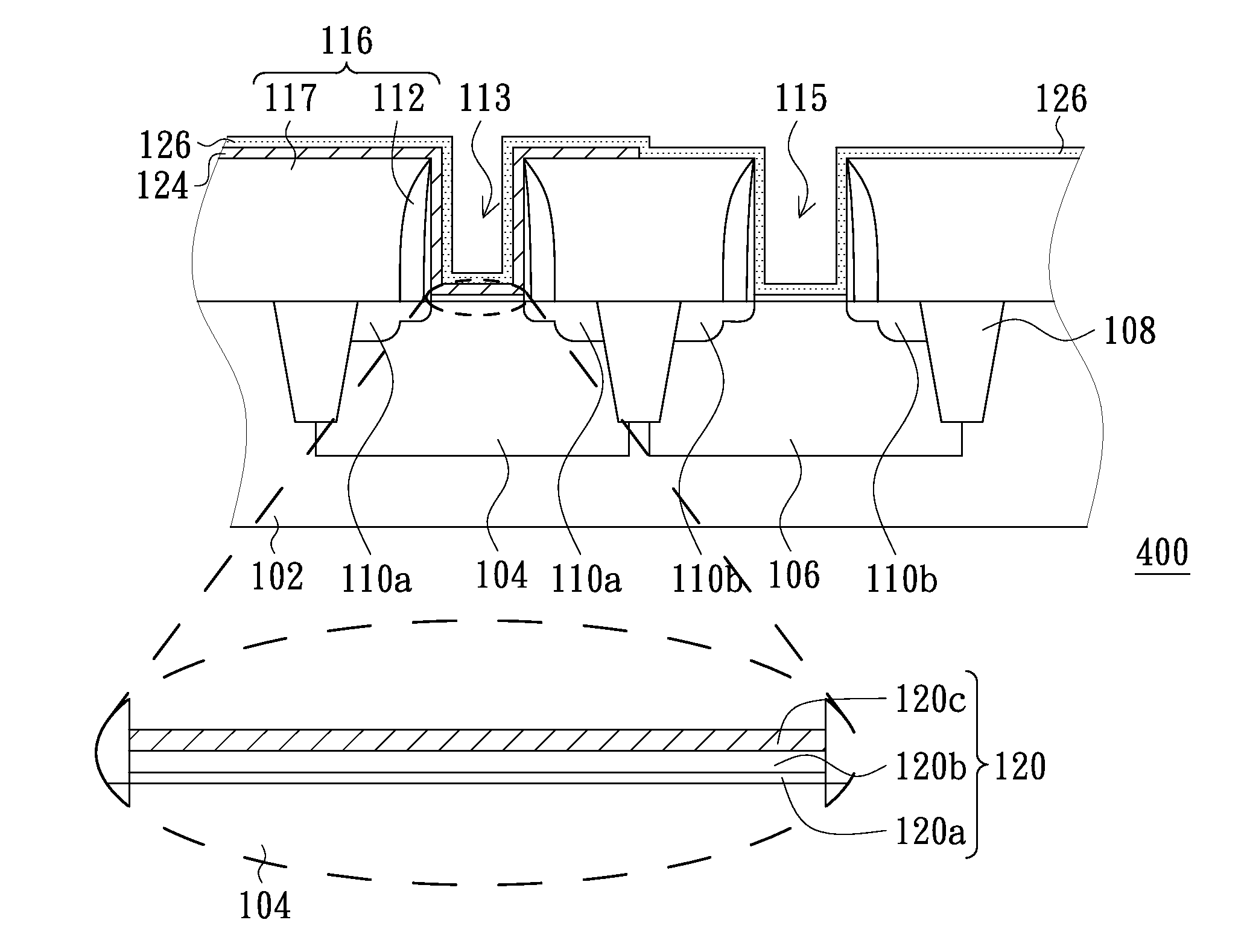
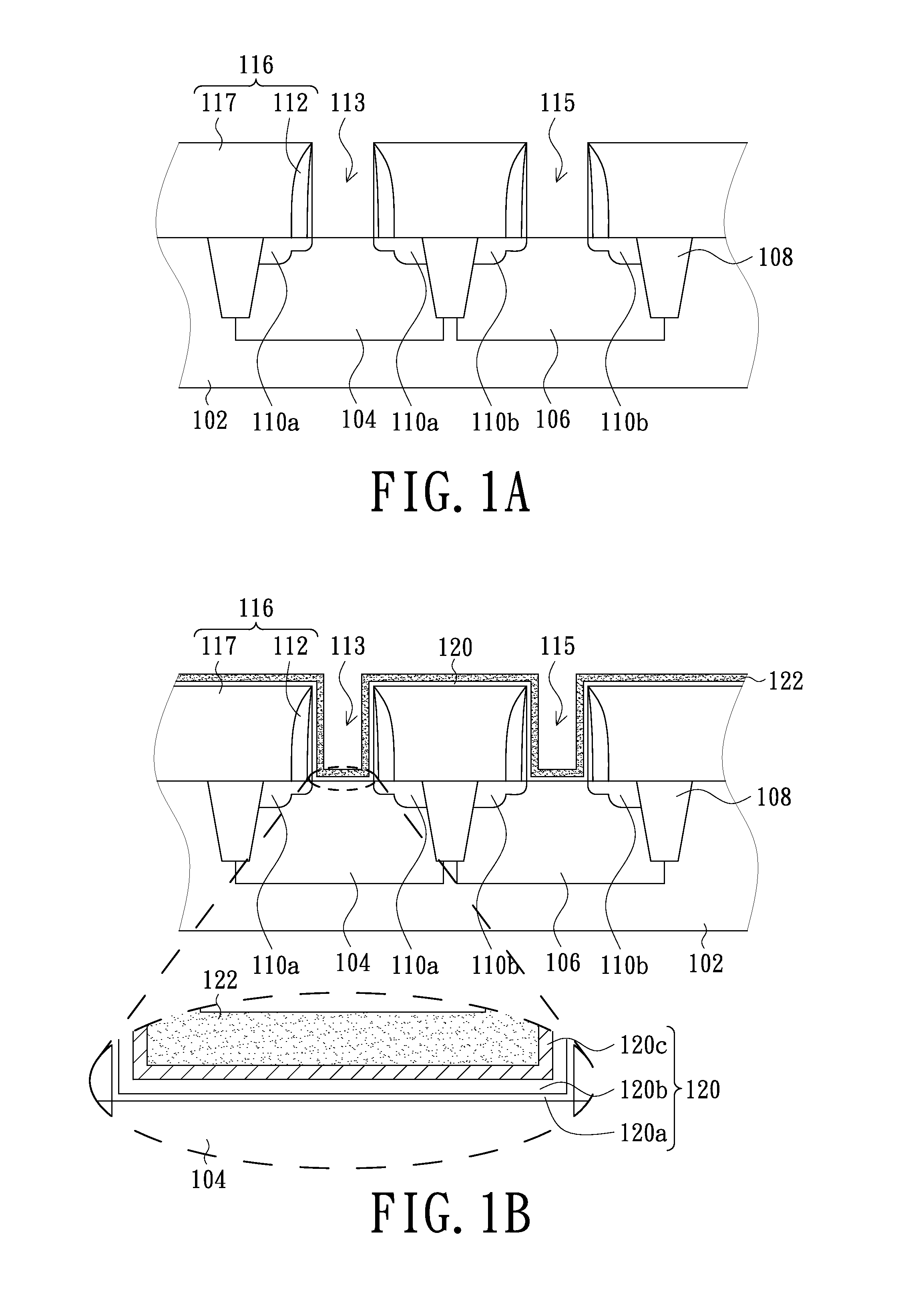
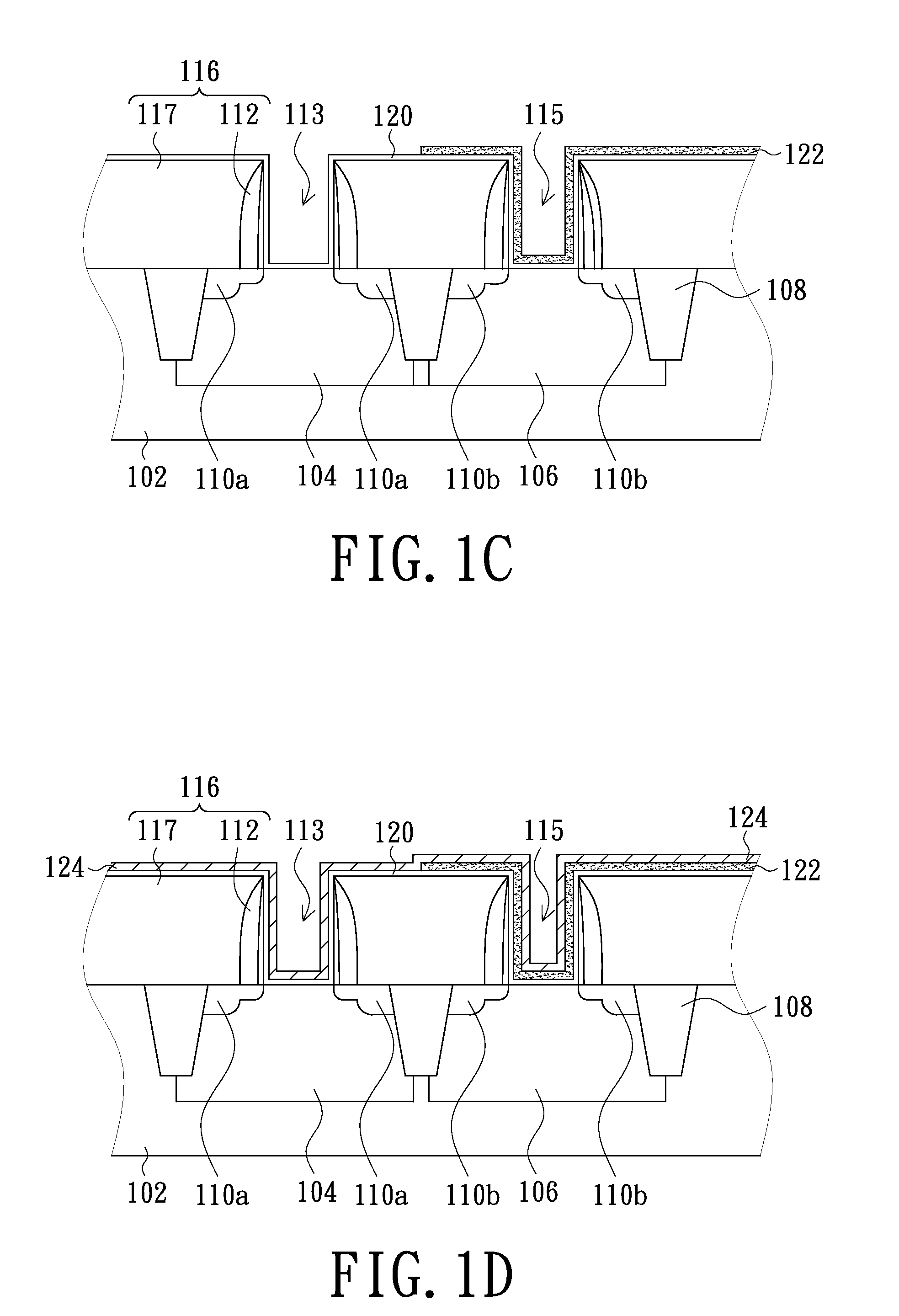
[0034]FIGS. 1A-1E illustrate cross-section views of a semiconductor structure during the fabricating process thereof according to an embodiment of the present invention. Referring to FIG. 1A, a substrate 112, such as a silicon substrate, a silicon-containing substrate, or a silicon-on-insulator (SOI) substrate, is pro...


PUM


Abstract

A fabricating method of semiconductor structure is provided. First, a substrate with a dielectric layer formed thereon is provided. The dielectric layer has a first opening and a second opening exposing a portion of the substrate. Further, a gate dielectric layer including a high-k dielectric layer and a barrier layer stacked thereon had been formed on the bottoms of the first opening and the second opening. Next, a sacrificial layer is formed on the portion of the gate dielectric layer within the second opening. Next, a first work function metal layer is formed to cover the portion of the gate dielectric layer within the first opening and the sacrificial layer. Then, the portion of the first work function metal layer and the sacrificial layer within the second opening are removed.

Description

BACKGROUND[0001]1. Field of the Invention[0002]The present invention relates to a semiconductor structure and a fabricating method thereof, and especially to a semiconductor structure and a fabricating method thereof which can improve the electrical performance of metal gate transistor.[0003]2. Description of Related Art[0004]In the field of semiconductor fabrication, the use of polysilicon material is diverse. Having a strong resistance for heat, polysilicon materials are commonly used to fabricate gate electrodes for metal-oxide semiconductor transistors. The gate pattern fabricated by polysilicon materials is also used to form self-aligned source / drain regions as polysilicon readily blocks ions from entering the channel region.[0005]However, devices fabricated by polysilicon still have many drawbacks. In contrast to most metal, polysilicon gates are fabricated by semiconductor materials having higher resistance, which causes the polysilicon gate to work under a much lower rate th...

Claims


Application Information

Patent Timeline
IPC IPC(8): H01L29/78H01L21/8234
CPCH01L21/28088H01L29/4966H01L29/513H01L29/517H01L21/823857H01L29/6659H01L29/7833H01L21/823842H01L29/66545
Inventor LIAO, DUAN-QUANCHEN, YI-KUNZHU, XIAO-ZHONG
Owner UNITED MICROELECTRONICS CORP
Why Eureka
Try Eureka