Metal-induced crystallization of continuous semiconductor thin films controlled by a diffusion barrier

Active Publication Date: 2013-02-28
THE BOARD OF TRUSTEES OF THE LELAND STANFORD JUNIOR UNIV
View PDF1 Cites 10 Cited by
  • Summary
  • Abstract
  • Description
  • Claims
  • Application Information

AI Technical Summary

Benefits of technology

[0009]According to one aspect of the invention, bias-voltage stressing of the GeOx layer controls the areal density of the crystalline Ge islands. In one aspect, the bias-voltage stressing includes applying an electric field between the Al seed layer and t

Problems solved by technology

This opens up the possibility of crystalline semiconductor deposition on flexible polymeric substrates, whereas a-Ge solid-phase crystallization requires temperatures significantly higher than 300° C. However, a-Ge/Al interfaces exhibit uncontrolled crystallization with growth of randomly orient

Method used


Image

  • Metal-induced crystallization of continuous semiconductor thin films controlled by a diffusion barrier
  • Metal-induced crystallization of continuous semiconductor thin films controlled by a diffusion barrier
  • Metal-induced crystallization of continuous semiconductor thin films controlled by a diffusion barrier

Examples


Embodiment Construction

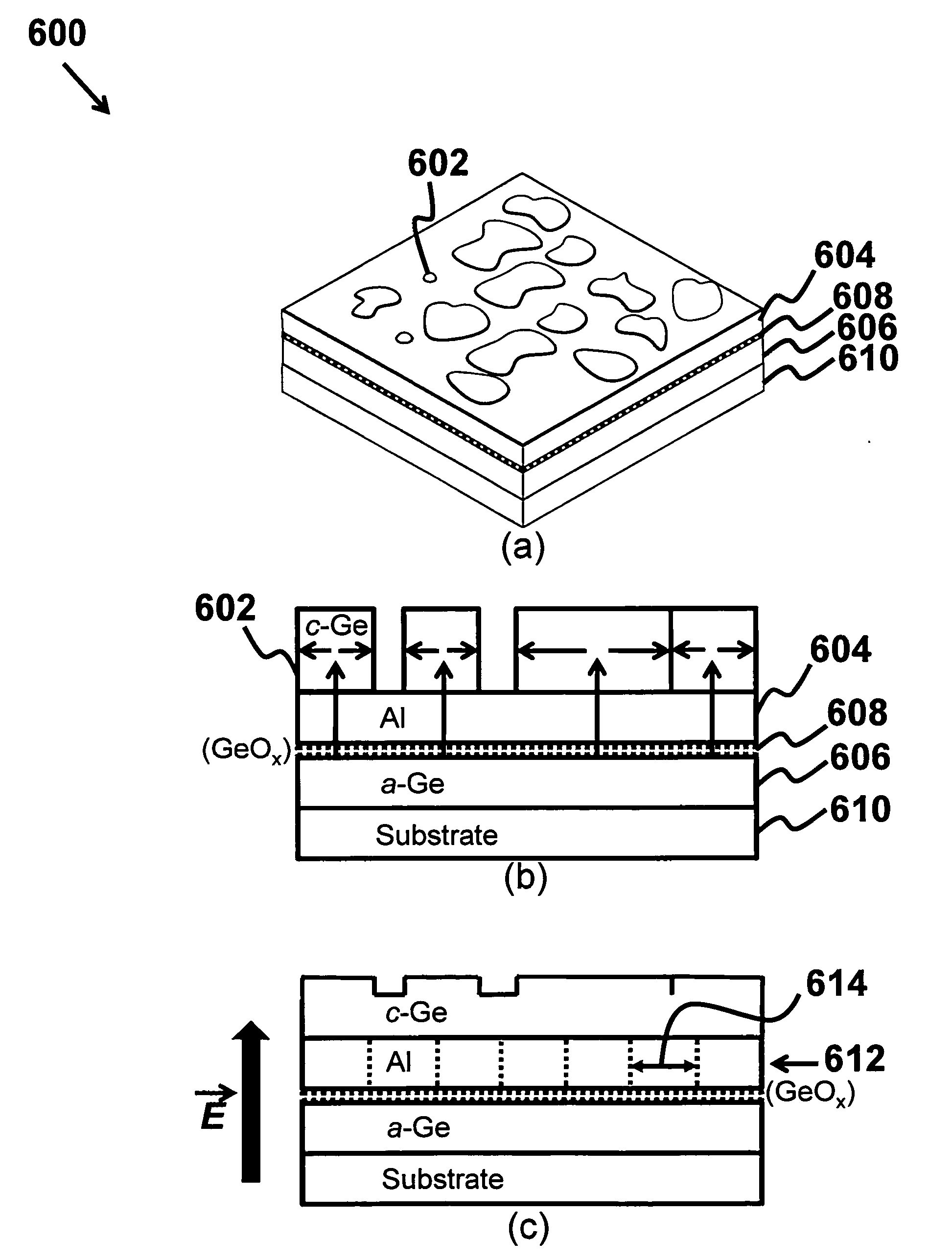
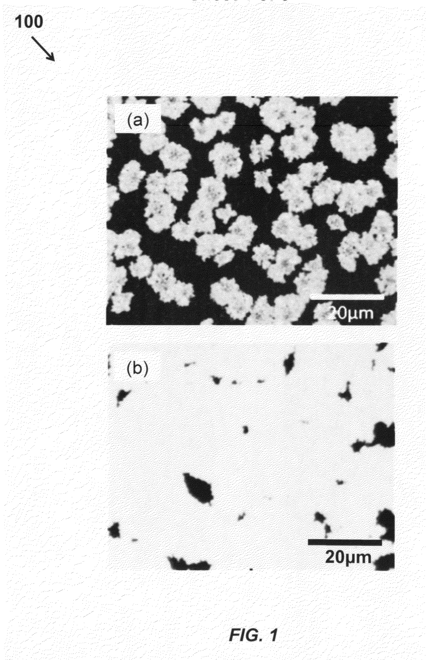
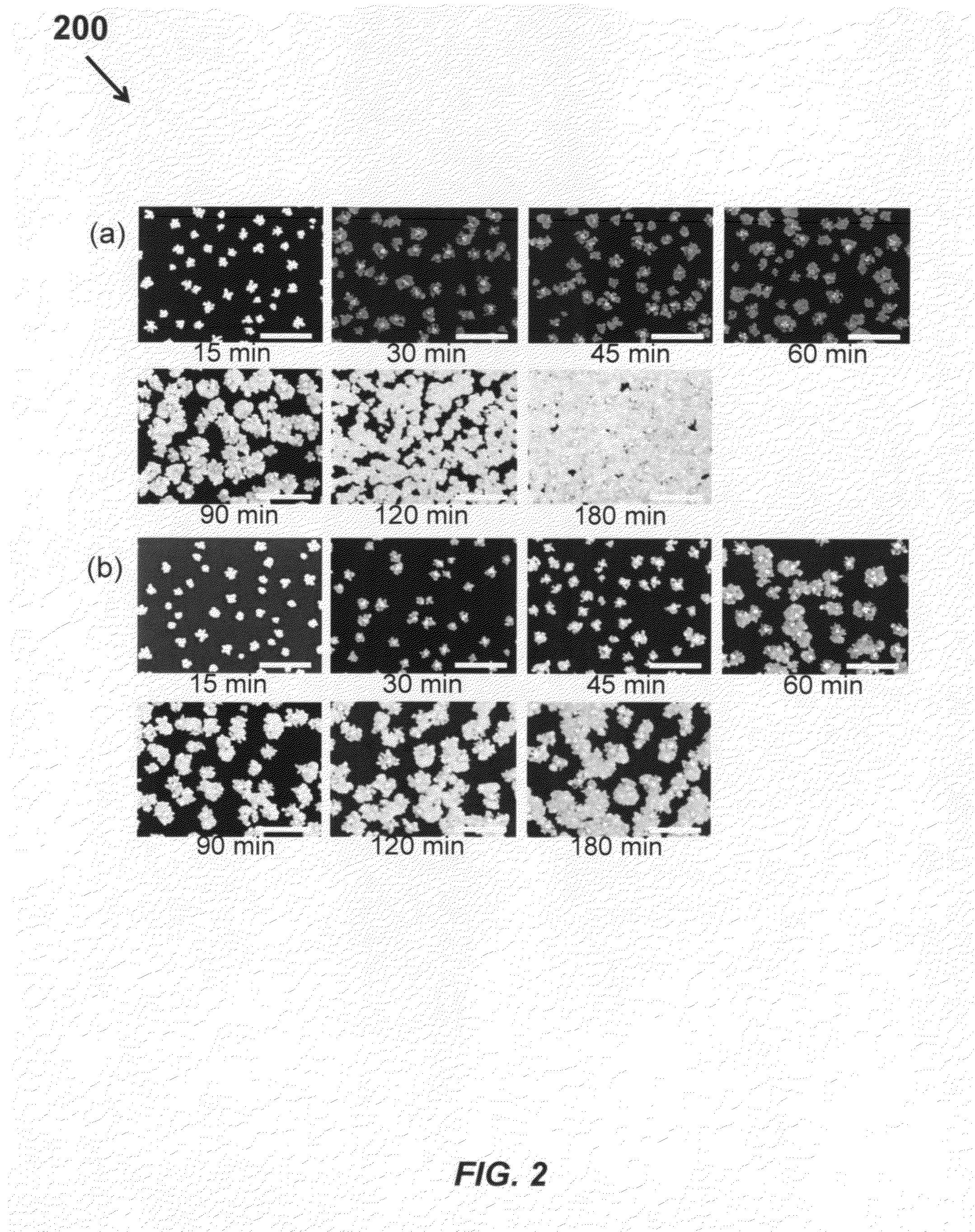
[0030]The current invention includes Al-seeded layer exchange crystallization to form poly-Ge thin films with micron-sized grains and (111)-preferred orientation at 200° C. A sub-nm GeOx (1


PUM


Abstract

A device and a method of forming a continuous polycrystalline Ge film having crystalline Ge islands is provided that includes depositing an amorphous Ge (a-Ge) layer on a substrate, oxidizing the top surface of the a-Ge layer to form a GeOx layer, depositing a seed layer of Al on the GeOx layer and catalyzing the Al seed layer, where Ge mass transport is generated from the underlying a-Ge layer to the Al seed layer through the GeOx layer by thermal annealing, where a continuous polycrystalline Ge film having crystalline Ge islands is formed on the Al seed layer.

Description

FIELD OF THE INVENTION[0001]The invention relates to growth of semiconductor thin films. More particularly, the invention relates to deposition of continuous polycrystalline Ge films having crystalline Ge island growth with preferred orientation.BACKGROUND OF THE INVENTION[0002]Low-temperature synthesis of polycrystalline germanium (poly-Ge) thin films is of great interest in thin-film photovoltaic and electronics applications. Low-temperature synthesis of polycrystalline semiconductor thin films (Si or Ge) on amorphous substrates has important applications in thin-film transistors and solar cells. Recently, (poly-Ge) thin films have been investigated as a low-cost substitute for single crystalline Ge substrates. Ge has good lattice matching with III-V semiconductors, and poly-Ge substrates have been shown to seed epitaxial growth of GaAs or Ge overlayers for polycrystalline single-junction or multijunction solar cell fabrication. Moreover, as-grown poly-Ge films can serve as buildi...

Claims


Application Information

Patent Timeline
IPC IPC(8): H01L29/04H01L21/20
CPCH01L21/02532H01L21/324H01L21/02672
Inventor HU, SHUMCINTYRE, PAUL C.
Owner THE BOARD OF TRUSTEES OF THE LELAND STANFORD JUNIOR UNIV
Why Eureka
Try Eureka