Semiconductor package structure and manufacturing method thereof

a technology of semiconductors and packaging, applied in the direction of semiconductor devices, semiconductor/solid-state device details, electrical apparatus, etc., can solve the problems of affecting reducing the reliability of the product, so as to achieve the effect of reducing the thickness of the package and improving reliability

Active Publication Date: 2013-02-28
CHIPMOS TECH INC
View PDF5 Cites 3 Cited by
  • Summary
  • Abstract
  • Description
  • Claims
  • Application Information

AI Technical Summary

Benefits of technology

[0008]Accordingly, the invention is directed to a semiconductor package structure with better reliability and smaller package thickness.

Problems solved by technology

When the count of chip contacts is ceaselessly increased and the chip area is made smaller and smaller with the development of semiconductor technology, it is difficult to re-distribute all contacts of a chip in area array scheme on the surface of the chip.
Even though a chip surface can accommodate all the contacts thereof, the interval between contacts still gets too small so as to affect the electrical reliability as the successive soldering process of solder balls.
However, it is easier to produce overflow during packaging, which leads the molding compound to extend onto a part of the active surface and increases the production fraction defective.
Further, the molding compound would contaminate the active surface of the chip so that the above-mentioned packaging scheme is unable to be used in CMOS chip.
As a result, the conventional scheme is unable to use vertical stacking method to package multiple semiconductor components (for example, multiple chips) in a same package structure.

Method used


Image

  • Semiconductor package structure and manufacturing method thereof
  • Semiconductor package structure and manufacturing method thereof
  • Semiconductor package structure and manufacturing method thereof

Examples


Embodiment Construction

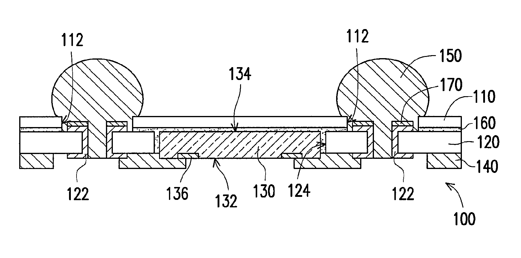
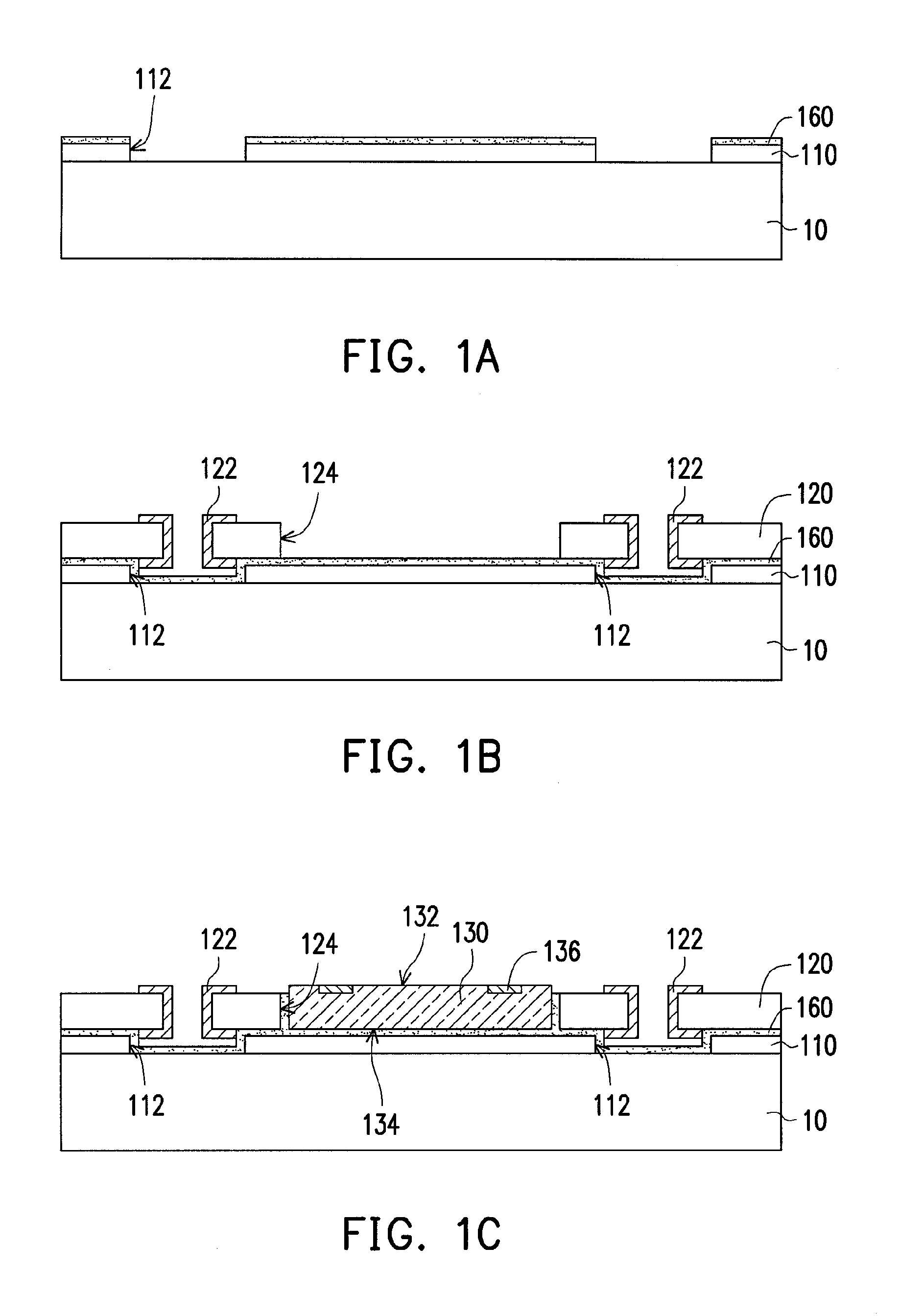
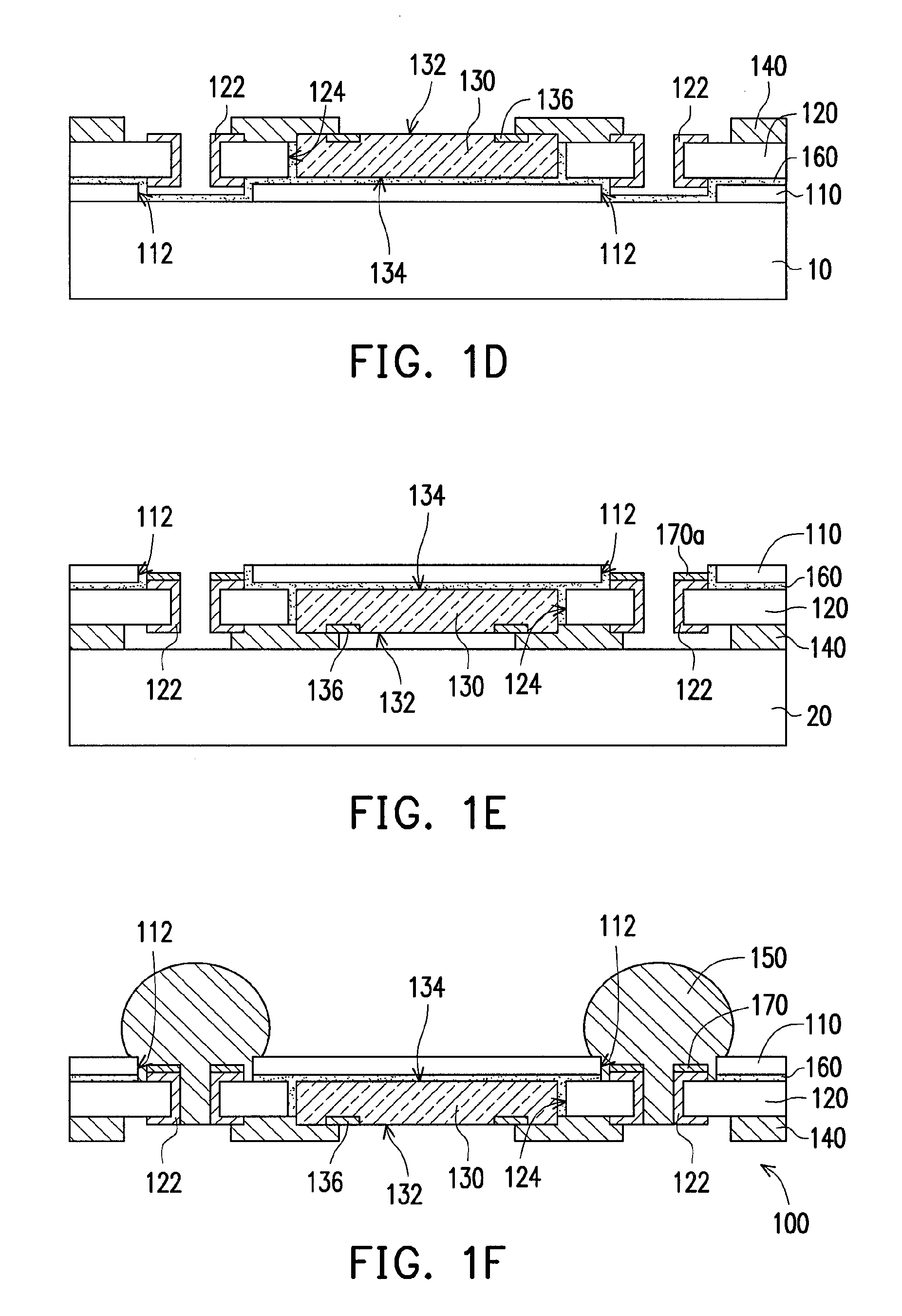
[0030]FIGS. 1A-1F are cross-sectional diagrams of a manufacturing method of semiconductor package structure according to an embodiment of the invention. Referring to FIG. 1A, the manufacturing method of semiconductor package structure of the embodiment includes following steps. First, a first carrier 10 and a first dielectric layer 110 are provided, in which the first dielectric layer 110 is disposed on the first carrier 10 and has a plurality of through holes 112. In the embodiment, the material of the first dielectric layer 110 is for example, bismaleimide-triazine resin (BT resin) and the method of forming the through holes 112 is, for example, laser drilling, mechanical drilling or punching. It should be noted that when the hardness of the first dielectric layer 110 is higher enough to serve as a supporting layer, the first carrier 10 can be saved. In other words, a user can optionally adopt the first carrier 10.

[0031]Next referring to FIG. 1A again, an adhesive layer 160 is for...


PUM


Abstract

A manufacturing method of semiconductor package structure includes: providing a first dielectric layer having multiple through holes; providing a second dielectric layer having multiple conductive vias and a chip-containing opening; laminating the second dielectric layer onto the first dielectric layer; disposing a chip in the chip-containing opening and adhering a rear surface of the chip onto the first dielectric layer exposed by the chip-containing opening; forming a redistribution circuit layer on the second dielectric layer wherein a part of the redistribution circuit layer extends from the second dielectric layer onto an active surface of the chip and the conductive vias so that the chip electrically connects the conductive vias through the partial redistribution circuit layer; forming multiple solder balls on the first dielectric layer wherein the solder balls are in the through holes and electrically connect the chip through the conductive vias and the redistribution circuit layer.

Description

CROSS-REFERENCE TO RELATED APPLICATION[0001]This application claims the priority benefit of Taiwan application serial no. 100130534, filed on Aug. 25, 2011. The entirety of the above-mentioned patent application is hereby incorporated by reference herein and made a part of this specification.BACKGROUND OF THE INVENTION[0002]1. Field of the Invention[0003]The invention generally relates to a semiconductor component and a manufacturing method thereof, and more particularly, to a semiconductor package structure and a manufacturing method thereof[0004]2. Description of Related Art[0005]The chip package is for protecting a bare die, reducing density of chip bonding spots and providing a chip with good heat-dissipating. When the count of chip contacts is ceaselessly increased and the chip area is made smaller and smaller with the development of semiconductor technology, it is difficult to re-distribute all contacts of a chip in area array scheme on the surface of the chip. Even though a c...

Claims


Application Information

Patent Timeline
Patent Type & Authority Applications(United States)
IPC IPC(8): H01L23/498H01L21/60
CPCH01L23/13H01L23/49816H01L23/49827H01L25/105H01L2224/16H01L2221/68345H01L2221/68363H01L2225/1041H01L2225/1058H01L21/6835
Inventor LIAO, TSUNG-JENPENG, MEI-FANGHUANG, CHENG-TANG
Owner CHIPMOS TECH INC
Why Eureka
Try Eureka