Combination ESD protection circuits and methods

a protection circuit and circuit technology, applied in the field of integrated circuits, can solve the problems of circuits that are not self-protecting, circuits may not be self-protecting, and other transistors may be damaged, etc., and achieve the effect of less tolerance and prone to esd events

Active Publication Date: 2013-02-28
MICRON TECH INC
View PDF2 Cites 31 Cited by
  • Summary
  • Abstract
  • Description
  • Claims
  • Application Information

AI Technical Summary

Problems solved by technology

Although some transistors may be capable of shunting some transient ESD current without damaging circuit components, other transistors may be damaged as a result of any ESD current at all.
In other words, some circuits may not be self-protecting.
Also, as semiconductor devices continue to shrink, they become more prone to and less tolerant of ESD events.
Once set, however, adjusting (e.g. changing, altering, etc.) the trigger condition, often requires redesign of the protection circuit.
Moreover, adding a dedicated ESD circuit may increase the capacitance seen at the input or output node, which may be unacceptable in high-speed I / O circuits.

Method used


Image

  • Combination ESD protection circuits and methods
  • Combination ESD protection circuits and methods
  • Combination ESD protection circuits and methods

Examples


Embodiment Construction

[0015]Certain details are set forth below to provide a sufficient understanding of embodiments of the invention. However, it will be clear to one skilled in the art that embodiments of the invention may be practiced without these particular details. Moreover, the particular embodiments of the present invention described herein are provided by way of example and should not be used to limit the scope of the invention to these particular embodiments. In other instances, well-known circuits, control signals, timing protocols, and software operations have not been shown in detail in order to avoid unnecessarily obscuring the invention.

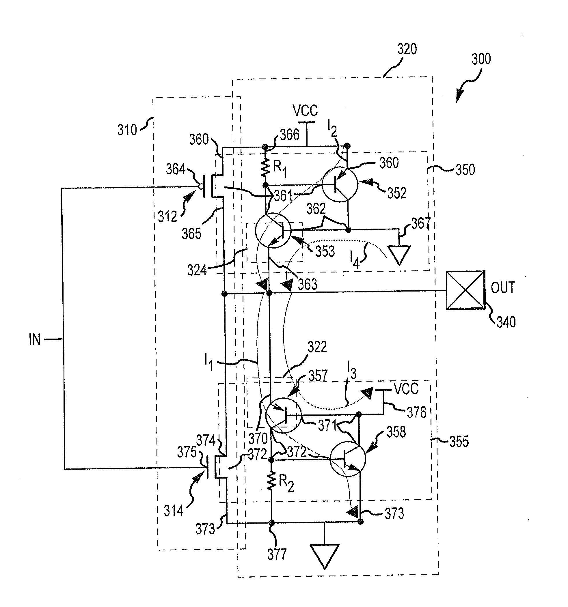
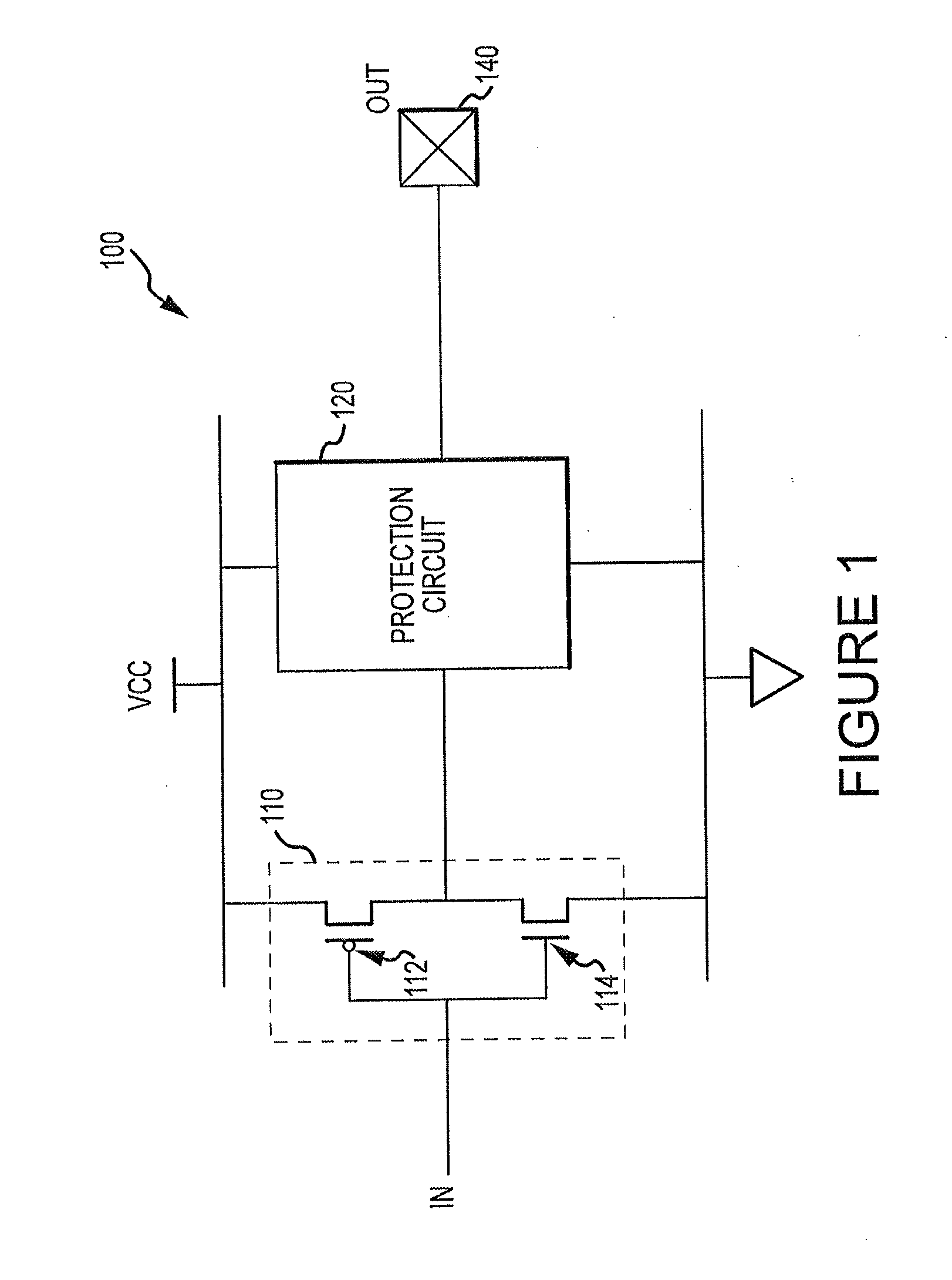
[0016]FIG. 1 illustrates an output circuit 100 according to an embodiment of the invention. The output circuit 100 includes a driver circuit 110 and a protection circuit 120. The output circuit 100 is configured to receive an input signal IN at an input node and provide an output signal OUT to an output node 140 responsive at least in part to the IN signal....


PUM


Abstract

Circuits, integrated circuits, apparatuses, and methods, such as those for protecting circuits against electrostatic discharge events are disclosed. In an example method, a thyristor is triggered to conduct current from a signal node to a reference voltage node using leakage currents provided by a transistor formed in a semiconductor doped well shared with the base of the thyristor. The leakage currents are responsive to a noise event (e.g., electrostatic discharge (ESD) event) at the signal node, and increase the voltage of the semiconductor doped well to forward bias the base and the collector of the thyristor. The triggered thyristor conducts the current resulting from the ESD event to the reference voltage node.

Description

TECHNICAL FIELD[0001]Embodiments of the invention relate generally to integrated circuits, and more particularly, in one or more of the illustrated embodiments, to circuitry combining an I / O driver with an electrostatic discharge protection device.BACKGROUND OF THE INVENTION[0002]Integrated circuits are connectable to “the outside world” through input nodes, output nodes, or input / output nodes such as bond pads, input pads, input / output pins, die terminals, die pads, contact pads, and so forth. Buffer circuitry, often configured as an inverter or a plurality of inverters, is interposed between such nodes and active circuitry of the integrated circuit. The buffer circuitry typically includes transistors which should be protected from over-limit electrical conditions, for example, voltages and / or currents caused by electrostatic discharge (ESD) during handling, testing and operation of the integrated circuit. Subjecting a device to ESD is referred to as an ESD event. An ESD event is a...

Claims


Application Information

Patent Timeline
Patent Type & Authority Applications(United States)
IPC IPC(8): H02H9/02H01L27/06
CPCH01L27/0617H01L27/0259H02H9/046H01L27/0817H01L27/0262H02H9/044
Inventor FAN, XIAOFENGCHAINE, MICHAEL D.
Owner MICRON TECH INC
Why Eureka
Try Eureka