System with a high power chip and a low power chip having low interconnect parasitics

Active Publication Date: 2013-03-07
NVIDIA CORP
View PDF7 Cites 29 Cited by
  • Summary
  • Abstract
  • Description
  • Claims
  • Application Information

AI Technical Summary

Benefits of technology

The present invention allows memory chips and other low-power devices to be placed close to high-power devices in the same integrated circuit system without getting too hot. This shortens the distance between the two types of devices, which improves performance and reduces interconnect issues.

Problems solved by technology

However, heat generated by higher-power chips is known to adversely affect memory chips and other devices positioned nearby.
Consequently, it is not thermally feasible to stack memory chips and passive devices directly on or under a CPU or other high-power chip when incorporated into a single IC package; such a configuration necessarily limits the power of the high-power chip or risks damage to and / or affects the performance of the memory chips.
Including lower-power chips in a single IC package by positioning such chips beside the high-power chips in the IC package is also undesirable, since such a horizontally distributed configuration results in the IC package having an impractically large footprint as well as having a longer interconnect path between the low-power chips and the high-power chips.

Method used


Image

  • System with a high power chip and a low power chip having low interconnect parasitics
  • System with a high power chip and a low power chip having low interconnect parasitics
  • System with a high power chip and a low power chip having low interconnect parasitics

Examples


Embodiment Construction

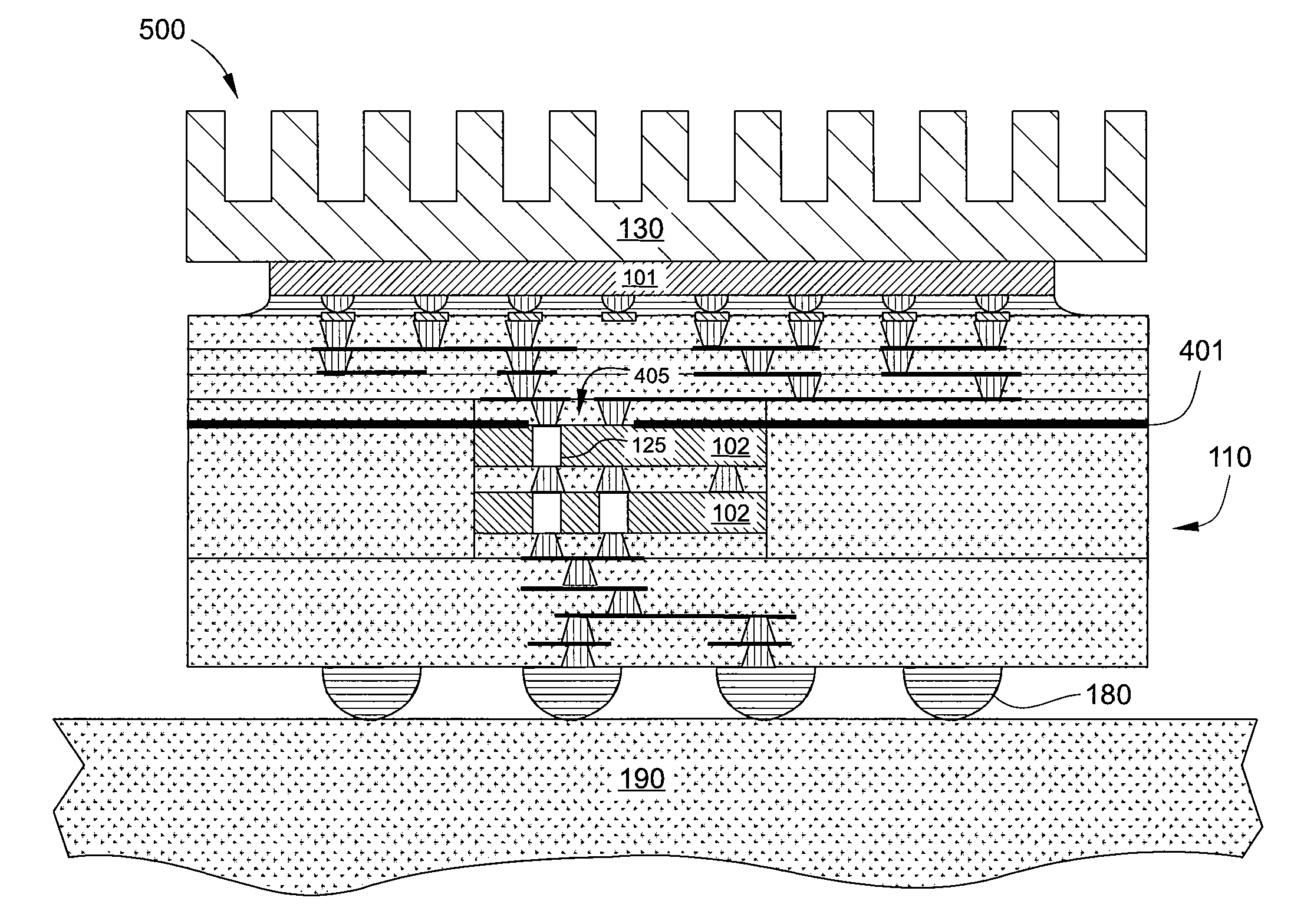
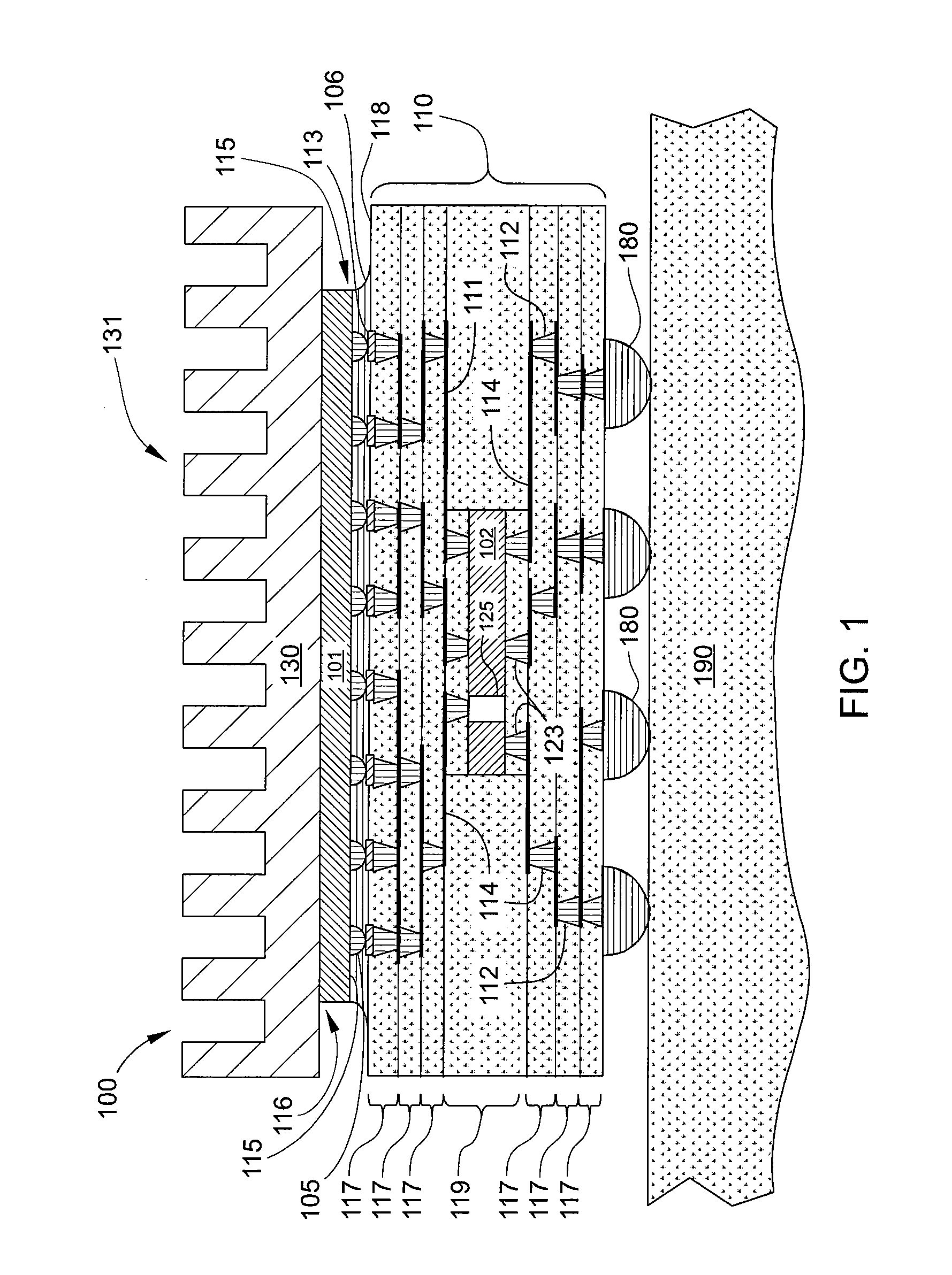
[0014]FIG. 1 is a schematic cross-sectional view of an integrated circuit (IC) system 100, according to one embodiment of the invention. IC system 100 includes multiple IC chips and / or other discrete microelectronic components, and is configured to electrically and mechanically connect said chips and components to a printed circuit board 190. IC system 100 includes a vertical combination, i.e., a stacked configuration, of a high-power chip 101 and a low-power chip 102, in which low-power chip 102 is thermally insulated from high-power chip 101 and therefore is not significantly affected by high-power chip 101.

[0015]IC system 100 includes high-power chip 101, low-power chip 102, a packaging substrate 110, and a plurality of packaging leads 180. High-power chip 101 is mounted on one side of packaging substrate 110 and low-power chip 102 is embedded in packaging substrate 110, so that low-power chip 102 is thermally insulated from high-power chip 101. Because portions of packaging subs...


PUM


Abstract

An IC system includes low-power chips, e.g., memory chips, located proximate one or more higher power chips, e.g., logic chips, without suffering the effects of overheating. The IC system may include a high-power chip disposed on a packaging substrate and a low-power chip embedded in the packaging substrate to form a stack. Because portions of the packaging substrate thermally insulate the low-power chip from the high-power chip, the low-power chip can be embedded in the IC system in close proximity to the high-power chip without being over heated by the high-power chip. Such close proximity between the low-power chip and the high-power chip advantageously shortens the path length of interconnects therebetween, which improves device performance and reduces interconnect parasitics in the IC system.

Description

BACKGROUND OF THE INVENTION[0001]1. Field of the Invention[0002]Embodiments of the present invention relate generally to integrated circuit chip packaging and, more specifically, to a system with a high power chip and a low power chip.[0003]2. Description of the Related Art[0004]In the packaging of integrated circuit (IC) chips, there is generally a trade-off between the thermal management of chips and other devices contained in a package and the performance of said devices. Specifically, by locating memory chips, passive devices, and other low-power components of an IC package as close as possible to the central processor unit (CPU) and other high-power devices in an IC package, communication between devices in the IC package is accelerated and packaging parasitics are reduced. However, heat generated by higher-power chips is known to adversely affect memory chips and other devices positioned nearby. Consequently, it is not thermally feasible to stack memory chips and passive devic...

Claims


Application Information

Patent Timeline
IPC IPC(8): H05K7/00
CPCH01L23/36H01L23/49822H01L2224/73253H01L2224/2518H01L23/3128H01L2225/06541H01L2225/06517H01L25/18H01L25/0657H01L2924/15311H01L23/49827H01L23/5389H01L25/0655H01L2224/16225H01L2224/32225H01L2224/73204H01L2924/00012H01L2224/04105H01L2224/12105H01L2225/1035H01L2225/1041H01L2225/1058H01L25/0652
Inventor YEE, ABRAHAM F.GRECO, JOEZHAI, JUNMINACAPELLI, JOSEPHCHEN, JOHN Y.
Owner NVIDIA CORP
Why Eureka
Try Eureka