Wafer dividing method

Active Publication Date: 2013-03-07
DISCO CORP
View PDF19 Cites 30 Cited by
  • Summary
  • Abstract
  • Description
  • Claims
  • Application Information

AI Technical Summary

Benefits of technology

[0005]However, when an external force is applied to the wafer to break the wafer along the modified layers, the modified layers are crushed to generate fine particles. Accordingly, there arises a problem such that the fine particles generated from the modified layers may stick to the surface of each devi

Problems solved by technology

However, when an external force is applied to the wafer to break the wafer along the modified layers, the modified layers are crushed to generate fine particles.
Accordingly, there arises a problem such that the fine particles generated from the

Method used


Image

  • Wafer dividing method
  • Wafer dividing method
  • Wafer dividing method

Examples


Embodiment Construction

1. First Preferred Embodiment

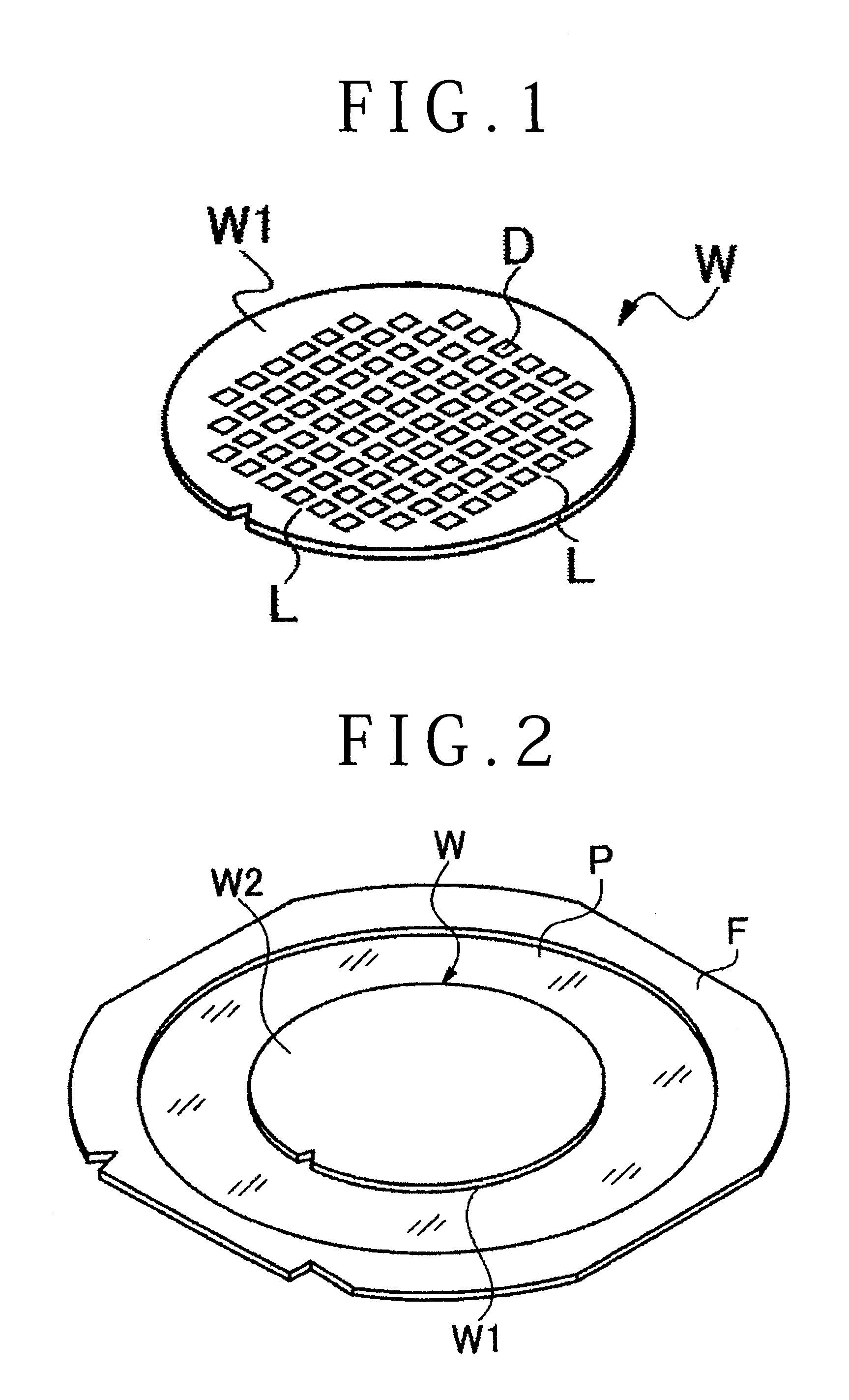
[0024]Referring to FIG. 1, there is shown a wafer W having a plurality of crossing division lines L formed on the front side W1, thereby partitioning a plurality of rectangular regions where a plurality of devices D are respectively formed.

(1) Protective Member Attaching Step

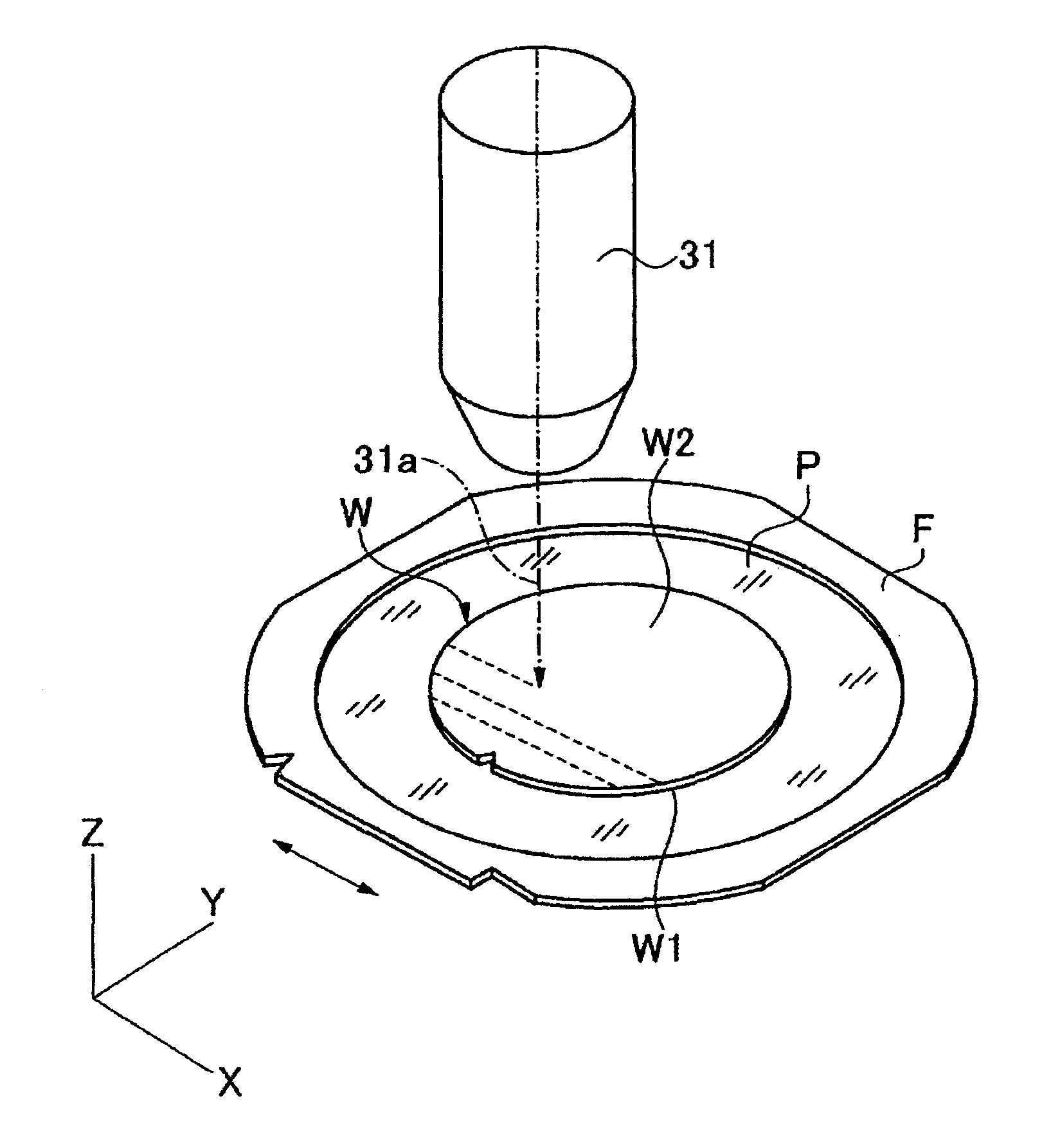
[0025]The wafer W is reversed from the condition shown in FIG. 1 and the front side W1 of the wafer W is attached to a protective member P such as an adhesive tape as shown in FIG. 2. A ring-shaped frame F is preliminarily attached to a peripheral portion of the protective member P. Thus, the wafer W is supported through the protective member P to the frame F. In this condition, the back side W2 of the wafer W is exposed.

(2) Modified Layer Forming Step

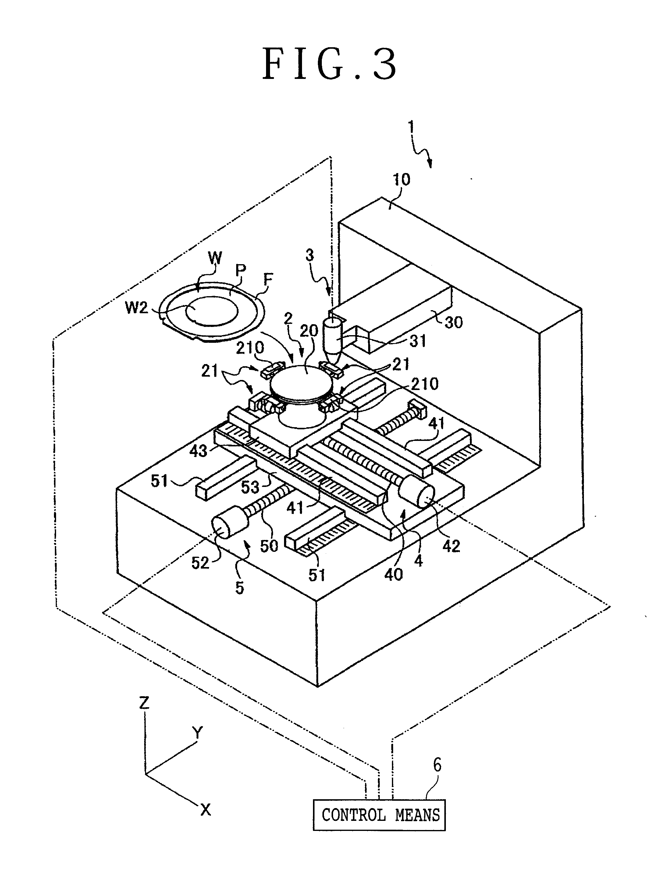
[0026]Thereafter, a laser beam is applied to the wafer W to form a modified layer inside the wafer W along each division line L. The modified layer can be formed by using a laser processing apparatus 1 shown in FIG. 3, for example. The ...


PUM

PropertyMeasurementUnit
Thicknessaaaaaaaaaa

Abstract

A wafer is divided by setting the focal point of a laser beam inside the wafer at positions corresponding to division lines, thereby forming modified layers inside the wafer along the division lines. Each modified layer has a thickness ranging from the vicinity of the front side of the wafer to the vicinity of the back side of the wafer. An etching gas or an etching liquid is supplied to the wafer to erode the modified layers, thereby dividing the wafer into individual devices. The modified layers are not crushed, so fine particles are not generated in dividing the wafer. Accordingly, fine particles do not stick to the surface of each device and cause a reduction in quality. Further, since the modified layers are removed by etching, it is possible to prevent a reduction in die strength of each device due to the remainder of the modified layers.

Description

BACKGROUND OF THE INVENTION[0001]1. Field of the Invention[0002]The present invention relates to a wafer dividing method of dividing a wafer into individual chips.[0003]2. Description of the Related Art[0004]A plurality of devices such as ICs and LSIs are formed on the front side of a wafer so as to be partitioned by a plurality of division lines. The wafer is divided into the individual devices by a cutting apparatus or a laser processing apparatus. These devices are widely used in various electrical equipment such as mobile phones and personal computers. As a method of dividing the wafer into the individual devices, there has been proposed and put into practical use a technique of applying a laser beam having a transmission wavelength to the wafer in the condition where the focal point of the laser beam is set inside the wafer at the positions corresponding to the division lines, thereby forming a plurality of modified layers inside the wafer along the division lines and next appl...

Claims


Application Information

Patent Timeline
IPC IPC(8): H01L21/78
CPCH01L21/78H01L21/30608H01L21/3065B28D5/00B23K26/0072B23K26/4075B23K2201/40B23K26/0057B23K26/367B23K26/40B23K26/364B23K26/53B23K26/3568B23K2101/40B23K2103/50
Inventor ARAI, KAZUHISA
Owner DISCO CORP
Why Eureka
Try Eureka