

Method for manufacturing electrodes and wires in gate last process
a gate electrode and gate last technology, applied in the field of gate electrode manufacturing and contact wire manufacturing in the gate last process, can solve the problems of increasing process complexity, cmp process brings lots of challenges to cmp technology, and plugs and metal gates also greatly increase the complexity of process integration, so as to simplify process integration and avoid defects. , the effect of strengthening the control of defects
- Summary
- Abstract
- Description
- Claims
- Application Information
AI Technical Summary
Benefits of technology
Problems solved by technology
Method used
Image

Examples
Embodiment Construction
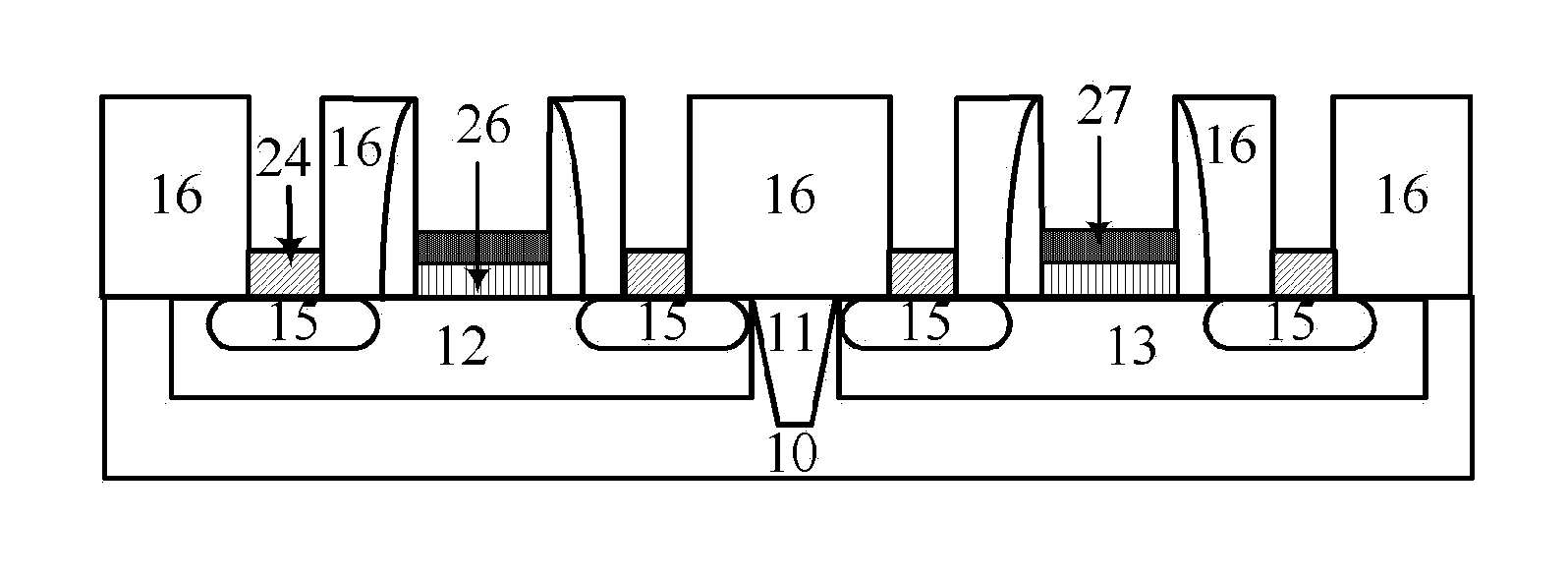
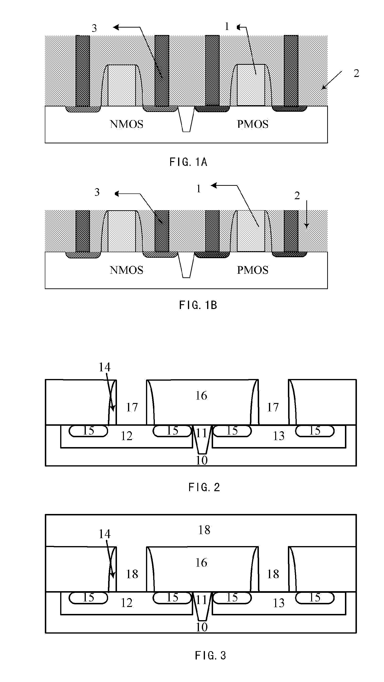
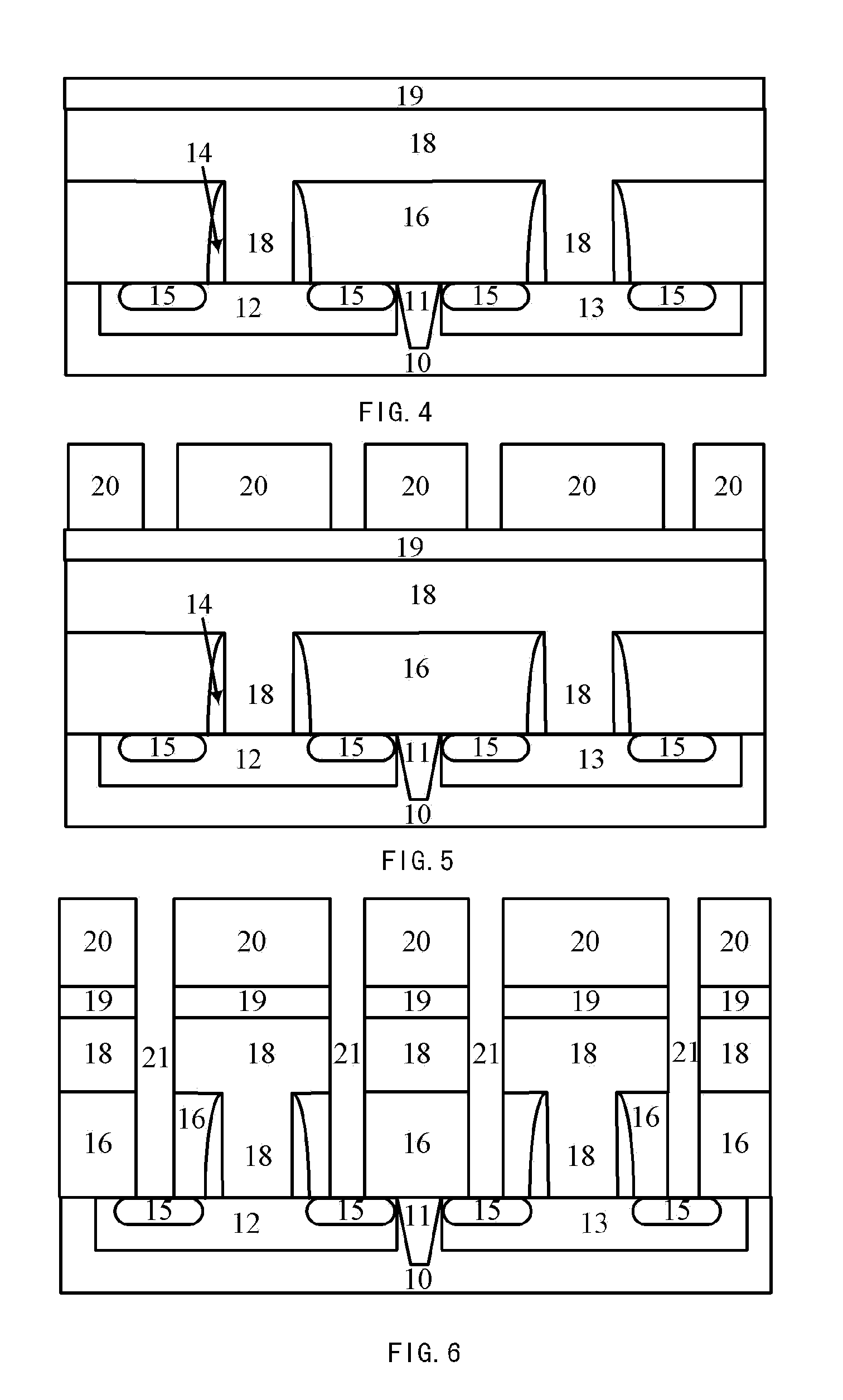
[0023]The features of the technical solutions and their technical effects of the present invention are described in detail with reference to the drawings in combination with the illustrative embodiments, and a method for manufacturing a gate electrode and a contact wire simultaneously in a gate last process is disclosed. It shall be pointed out that like reference signs indicate like structures.
[0024]First, referring to FIG. 2, a known gate last process is used to form a basic structure including gate trenches. An NMOS well region 12 and a PMOS well region 13 are formed respectively by well region ion implantation into a substrate 10 including an isolator 11. Then a pad layer and a dummy gate material layer (not shown) are deposited in turn on the well regions and etched to form a dummy gate stack structure. Next spacers 14 are formed by depositing and etching on the dummy gate stack structure. Source / drain regions 15 are formed by source / drain ion implantation with the spacers as a...
PUM
 Abstract
Description
Claims
Application Information