Thin film solar cells and manufacturing method thereof

a solar cell and thin film technology, applied in the direction of basic electric elements, electrical equipment, semiconductor devices, etc., can solve the problems of significant recombination loss of a photogeneration carrier, fatal defect of serious degradation of hydrogenated amorphous silicon (a-si:h), and limit to achieve high efficiency, etc., to achieve high hydrogen dilution and high hydrogen dilution

Inactive Publication Date: 2013-03-14
KISCO CORP (KR)
View PDF0 Cites 19 Cited by
  • Summary
  • Abstract
  • Description
  • Claims
  • Application Information

AI Technical Summary

Benefits of technology

[0016]One aspect of the present invention is a thin film silicon solar cell including: a front transparent electrode stacked on a transparent insulating substrate; a p-type layer stacked on the front transparent electrode; an i-type photoelectric conversion layer stacked on the p-type layer; an n-type layer stacked on the i-type photoelectric conversion layer; and a metal back electrode layer stacked on the n-type layer. The n-type layer includes: an n-type amorphous silicon first n layer which is stacked on the i-type photoelectric conversion layer and has a thickness of 3 nm to 7 nm; and an n-type silicon second n layer which is stacked on the first n layer and has a thickness of 15 nm to 30 nm and is more highly hydrogen-diluted than the first n layer.
[0017]Another aspect of the present invention is a thin film silicon solar cell i

Problems solved by technology

That is to say, the hydrogenated amorphous silicon (a-Si:H) has a fatal defect of being seriously degraded by light irradiation.
However, an abrupt hetero-junction of a p-type layer and an i-type layer (p-a-SiC:H/i-a-Si:H) increases defect density at the interface, thereby causing significant recombination loss of a photogeneration carrier.
Therefore, there is a limit to achieve a high efficiency.
However, because a dangling bond

Method used


Image

  • Thin film solar cells and manufacturing method thereof
  • Thin film solar cells and manufacturing method thereof
  • Thin film solar cells and manufacturing method thereof

Examples


Embodiment Construction

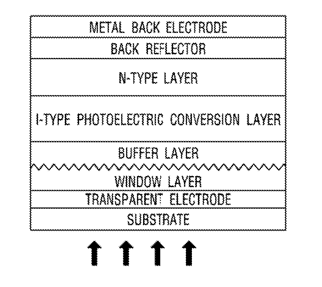
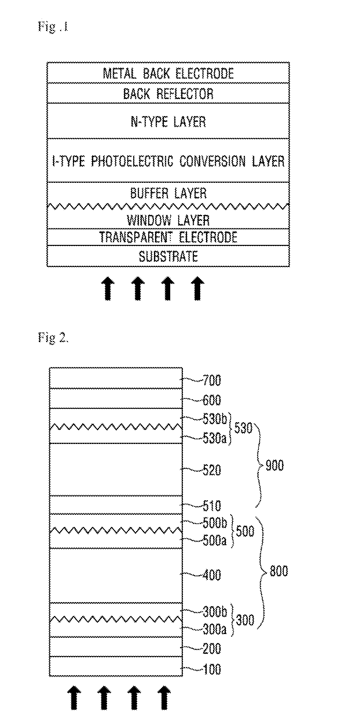
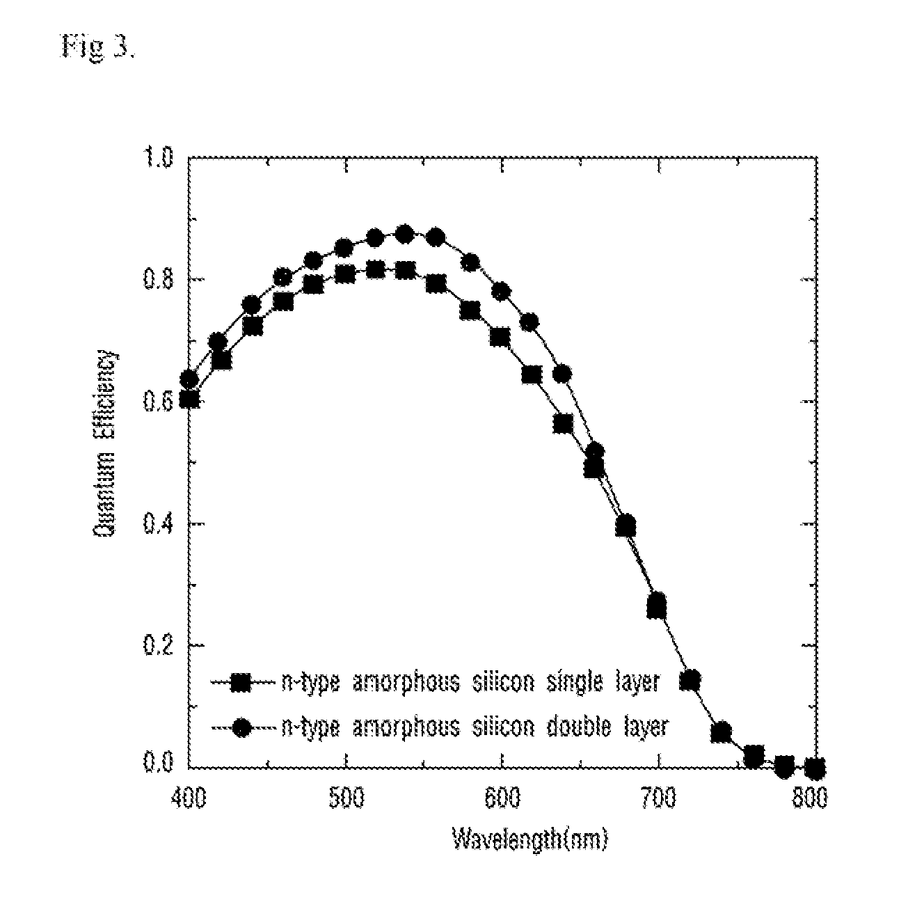
[0027]The following detailed description of the present invention shows a specified embodiment of the present invention and will be provided with reference to the accompanying drawings. The embodiment will be described in enough detail that those skilled in the art are able to embody the present invention. It should be understood that various embodiments of the present invention are different from each other and need not be mutually exclusive. For example, a specific shape, structure and properties, which are described in this disclosure, may be implemented in other embodiments without departing from the spirit and scope of the present invention with respect to one embodiment. Also, it should be noted that positions or placements of individual components within each disclosed embodiment may be changed without departing from the spirit and scope of the present invention. Therefore, the following detailed description is not intended to be limited. If adequately described, the scope of...


PUM


Abstract

A thin film silicon solar cell including: a front transparent electrode stacked on a transparent insulating substrate; a p-type layer stacked on the front transparent electrode; an i-type photoelectric conversion layer stacked on the p-type layer; an n-type Saver stacked, on the i-type photoelectric conversion layer; and a metal back electrode layer stacked on the n-type layer, wherein the n-type layer includes: an n-type amorphous silicon first n layer which is stacked on the i-type photoelectric conversion layer and has a thickness of 3 nm to 7 nm; and an n-type silicon second n layer which is stacked on the first n layer and has a thickness of 15 nm to 30 nm and is more highly hydrogen-diluted than the first n layer.

Description

CROSS-REFERENCE TO RELATED APPLICATIONS[0001]This application claims the benefit of Korean Patent Application No. 10-2011-0092018, filed Sep. 9, 2011, the entirety of which is hereby incorporated by reference.FIELD OF THE INVENTION[0002]This embodiment relates to a thin film silicon solar cell and a manufacturing method thereof, and more particularly to a thin film silicon solar cell, which has improved photoelectric conversion efficiency, and a manufacturing method thereof.BACKGROUND OF THE INVENTION[0003]An amorphous silicon (a-Si) solar cell was first developed in 1976 and has been being researched because hydrogenated amorphous silicon (a-Si:H) has a high photosensitivity in the visible light region, easiness to adjust an optical band gap, and a large area processability at a low cost and low temperature.[0004]However, it was discovered that the hydrogenated amorphous silicon (a-Si:H) has Stabler-Wronski effect. That is to say, the hydrogenated amorphous silicon (a-Si:H) has a f...

Claims


Application Information

Patent Timeline
IPC IPC(8): H01L31/075
CPCH01L31/075Y02E10/548H01L31/076H01L31/0445H01L31/18
Inventor MYONG, SEUNG-YEOPJEON, LA-SUN
Owner KISCO CORP (KR)
Why Eureka
Try Eureka