Light emitting diode with conformal surface electrical contacts with glass encapsulation

a technology of light-emitting diodes and conformal surfaces, applied in semiconductor/solid-state device manufacturing, semiconductor devices, electrical apparatus, etc., can solve the problems of silicone and epoxy, high-efficiency encapsulation challenges, and wire bonding standard electrical contact of leds that cannot be manufactured, etc., to achieve long-life leds, prevent failures, and high efficiency

Inactive Publication Date: 2013-03-21
RGT UNIV OF CALIFORNIA
View PDF0 Cites 92 Cited by
  • Summary
  • Abstract
  • Description
  • Claims
  • Application Information

AI Technical Summary

Benefits of technology

[0015]Therefore, the present invention also describes a novel way of electrically contacting LEDs with conformal metal surface contacts before subsequently encapsulating the LEDs with a high refractive index glass, or glass preform with a high index intermediate medium. Side contacts may require an insulator to be deposited below the metal contact to prevent electrical shorting of the LED along the sidewall. The use of conformal contacts allows the removal of traditional wire bonds, preventing failures during high temperature encapsulation (especially if refractory metals are used for the contacts).
[0016]Currently LEDs are electrically contacted via gold wire bonds or backside bump solder bonds (in the case of flip chips). These wire bonds are suitable for currently used encapsulation media, usually silicone or epoxy based materials, which cure at relatively low temperatures (less than 200° C.). Both silicone and epoxy, however, present challenges for encapsulation of high efficiency, long lifetime LEDs. Epoxies develop a yellow color with exposure to UV light and so over the long lifetime of LEDs, the yellowing of the encapsulant decreases the optical transparency and the light output power decreases. Silicones are not rigid and can delaminate from LEDs, destroying the wire bonds under certain operating conditions. Both of the current encapsulants are also limited to fairly low refractiv

Problems solved by technology

Standard electrical contacting of LEDs by wire bonding does not allow such fabrication due to the differences in coefficients of thermal expansion (CTEs) between glass, semiconductors, and metal wires.
Both silicone and epoxy, however, present challenges for encapsulation of high efficiency, long lifetime LEDs.
Silicones are not rigid and can dela

Method used


Image

  • Light emitting diode with conformal surface electrical contacts with glass encapsulation
  • Light emitting diode with conformal surface electrical contacts with glass encapsulation
  • Light emitting diode with conformal surface electrical contacts with glass encapsulation

Examples


example

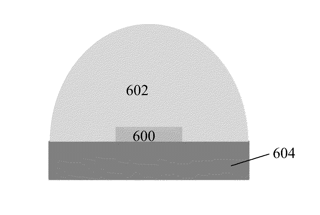
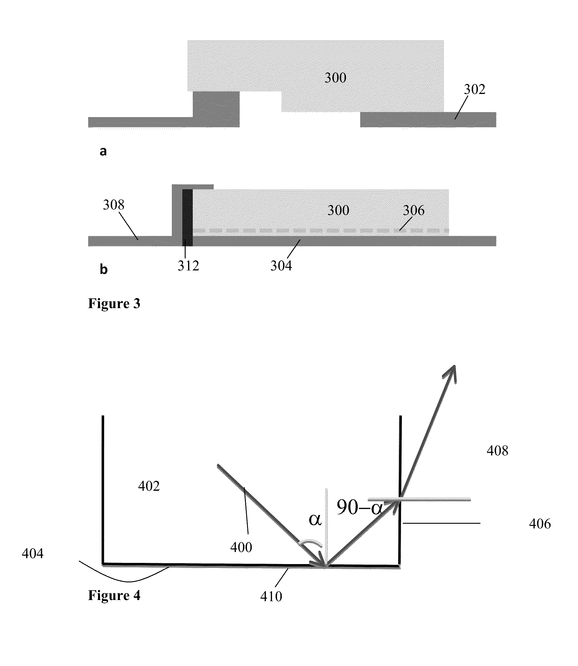
[0127]The preferred method is a deposition of the conformal metal contacts 202 over a sidewall 212 that has previously been coated by a low optical loss dielectric 204. For high temperature encapsulation of LEDs, a refractory metal, such as tungsten, is preferable for the conformal metal contacts 202, to prevent damage to the contacts 202 during encapsulation with glass. Ideally, full glass encapsulation can be achieved on a header, with the glass being deposited in a fashion similar to that of current epoxy and silicone encapsulants (e.g., by injection molding, frit reflow or other molding methods). In the case where the LEDs cannot be subjected to the high temperatures of the glass, or glass functionality is not able to be achieved with direct molding, glass preforms can be created with the desired package dimensions and functionality, and bonded to the LED with an intermediate medium 508 (where the intermediate medium may be comprised of a silicone, epoxy, sol-gel glass or simila...


PUM


Abstract

An optoelectronic device (e.g., LED) comprising one or more conformal surface electrical contacts conforming to surfaces of the device; and a high refractive index glass partially or totally encapsulating the device and the conformal surface electrical contacts, wherein traditional wire bonds and/or bond pads are not used and the glass is a primary encapsulant for the device.

Description

CROSS-REFERENCE TO RELATED APPLICATIONS[0001]This application claims the benefit under 35 U.S.C Section 119(e) of U.S. Provisional Patent Application Ser. No. 61 / 536,837 filed on Sep. 20, 2011, by James S. Speck, Claude Weisbuch, Nathan Pfaff, Leah Kuritzky, and Christopher Lalau Keraly, entitled “LIGHT EMITTING DIODE WITH CONFORMAL SURFACE ELECTRICAL CONTACTS WITH GLASS ENCAPSULATION,” attorney's docket number 30794.427-US-P1 (2012-121-1), which application is incorporated by reference herein.[0002]This application is related to the following co-pending and commonly-assigned applications:[0003]U.S. Utility patent application Ser. No. 12 / 275,136, filed on Nov. 20, 2008, by Steven P. DenBaars, Shuji Nakamura and Hisashi Masui, entitled “HIGH LIGHT EXTRACTION EFFICIENCY PACKAGE FOR A LIGHT EMITTING DIODE,” attorney's docket number 30794.290-US-I1 (2007-271), which application is a continuation-in-part of U.S. Utility patent application Ser. No. 11 / 940,872, filed on Nov. 15, 2007, by S...

Claims


Application Information

Patent Timeline
IPC IPC(8): H01L33/08H01L33/48H01L33/50
CPCH01L33/385H01L33/507H01L33/56H01L33/62H01L2924/0002H01L2924/00H01L2224/16H01L2224/48463H01L2224/49107H01L2924/10155H01L2224/45144
Inventor SPECK, JAMES S.WEISBUCH, CLAUDE C. A.PFAFF, NATHANKURITZKY, LEAHKERALY, CHRISTOPHER LALAU
Owner RGT UNIV OF CALIFORNIA
Why Eureka
Try Eureka