Encapsulation structure for silicon pressure sensor

a technology of encapsulation structure and pressure sensor, which is applied in the direction of fluid pressure measurement, acceleration measurement using interia forces, instruments, etc., can solve the problems of complex structure and manufacturing process, inability to meet the needs of batch production and application of silicon pressure sensors, and high cost, so as to reduce material and process costs and simplify the encapsulation structure and manufacturing process.

Active Publication Date: 2013-03-21
ZHOU JINGXUN
View PDF0 Cites 3 Cited by
  • Summary
  • Abstract
  • Description
  • Claims
  • Application Information

AI Technical Summary

Benefits of technology

[0016](1) The bonding technique is eliminated and there is no silicon oil or convoluted diaphragm for separation, so this invention simplifies the encapsulation structure and manufacturing process which greatly reduces the cost of material and process.
[0017](2) The circuit forms on the top of the case with the function of PCB substrate and is electrically connected to signal conditioning chip. Thus it is more convenient to make pressure transferring modules with standard signal output.
[0018](b 3) The sealing pad is made of flexible material which keeps the pressure sensing chip floating in the ceramic space so as to protect from rigid encapsulation stress.
[0019](4) There is backup washer with certain thickness on top of pressure sensing chip or at the bottom of the case so as to protect the pressure sensing chip from being destroyed. Meanwhile the sensing chip can resist more than ten times of pressure overloading and so has the overloading ability.

Problems solved by technology

However, as for this kind of encapsulation, the structure and manufacturing process is complicated and the cost is high.
So it can't meet the needs of batch production and application of silicon pressure sensors.

Method used


Image

  • Encapsulation structure for silicon pressure sensor
  • Encapsulation structure for silicon pressure sensor
  • Encapsulation structure for silicon pressure sensor

Examples


first embodiment

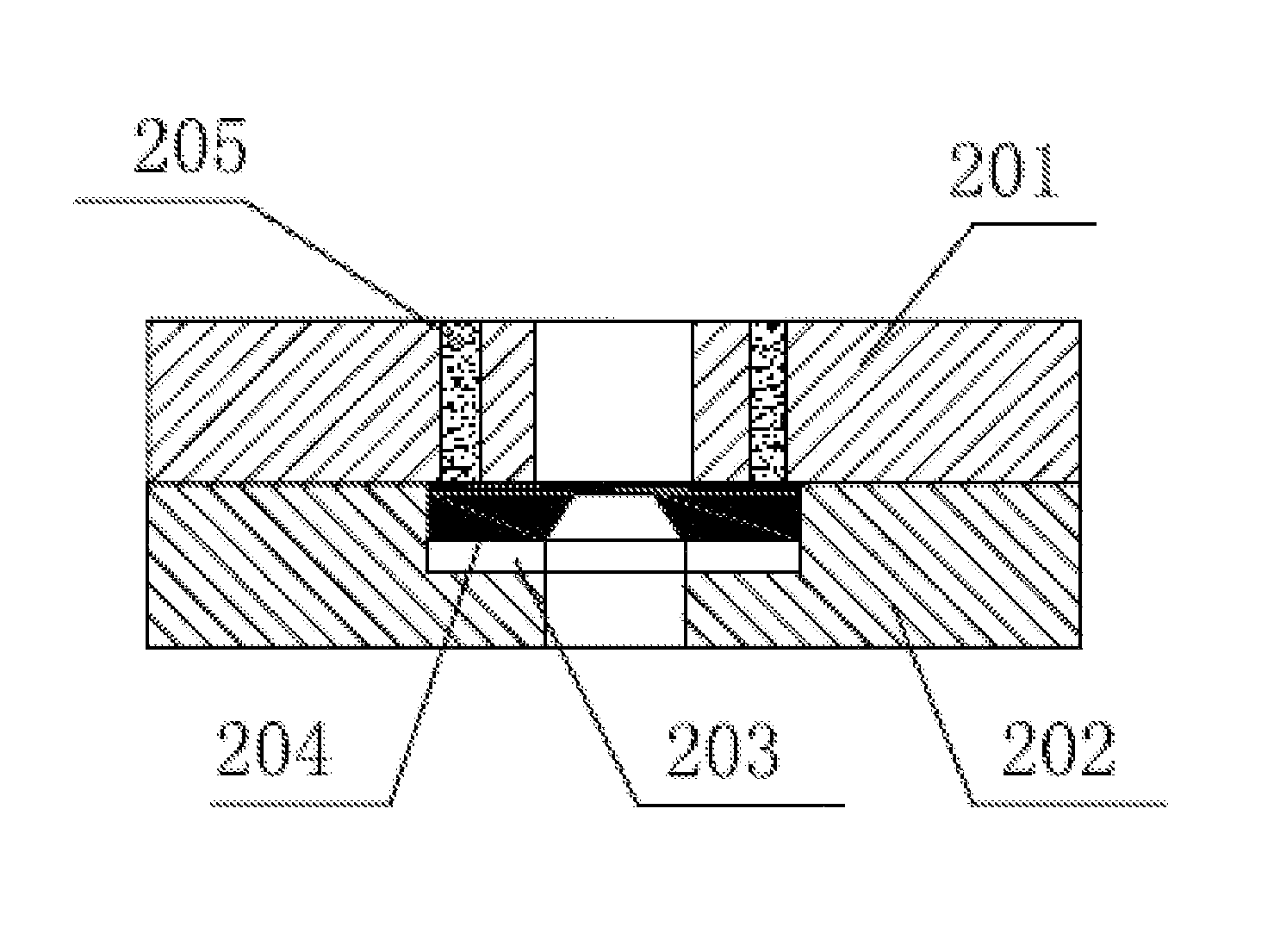
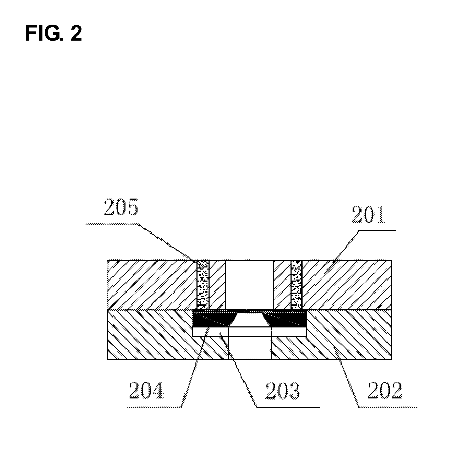
[0030]FIG. 2 is a schematic diagram for the first embodiment. Referring to FIG. 2, case 201 and stem 202 are bonded together as a carrier, and form a cavity therebetween. Sealing pad 203 and pressure sensing chip 204 are placed in the cavity with sealing pad 203 beneath the pressure sensing chip 204. The bonding pad of pressure sensing chip 204 is connected to the external circuit through case 201. One preferred option is that, case 201 has through holes in the corresponding position of the bonding pad of pressure sensing chip 204. The through holes are filled with conductive adhesive 205 so as to transfer the signal of the bonding pad to the top the case 201 which is connected to the exterior circuits. In this embodiment, sealing pad 203 is made of flexible material (e.g. rubber) which keeps pressure sensing chip 204 floating in the cavity so as to protect it from rigid encapsulation stress.

[0031]Second Embodiment

[0032]As one further preferred option as shown in FIG. 3, case 201 ha...

fourth embodiment

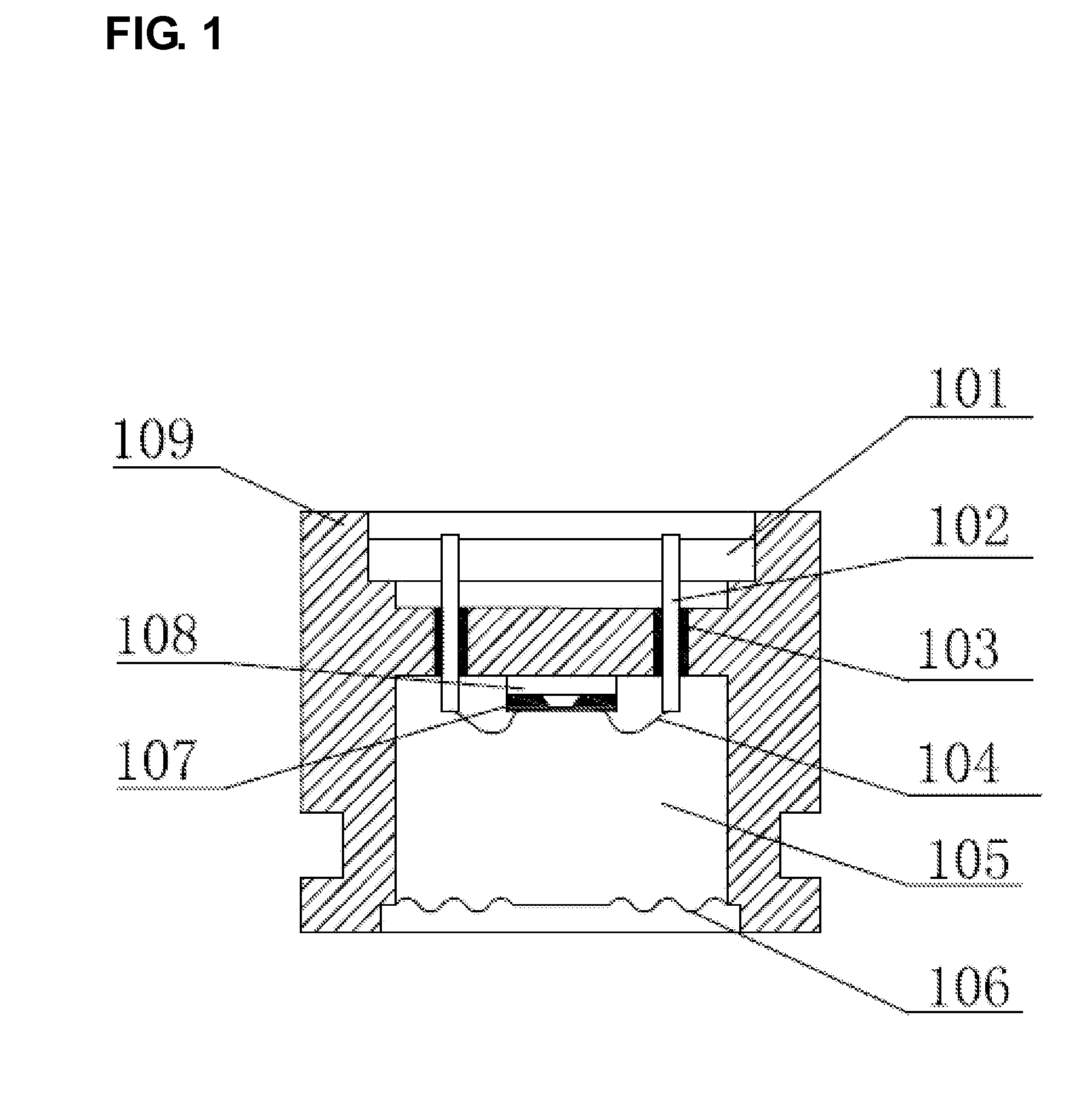
[0035]As one further preferred option as shown in FIG. 5, case 201 has through wires 207 in it which are connected to conducting strips on their both ends. The bonding pad of pressure sensing chip 204 is connected to one of the conducting strips and then the signal of the bonding pad is transferred to the top of case 201 which is connected to the exterior circuits through conducting strips and wires 207.

[0036]On the basis of the four above-mentioned embodiments, there can be further embodiments as follows.

fifth embodiment

[0037]As one further preferred option, as shown in FIG. 6, it forms circuits on top of case 201 by thick-film or thin-film process. Meanwhile, it has the function as PCB substrate which is electrically connected to signal conditioning chip 208. Thus it is the encapsulation structure for silicon pressure sensors with standard signal output.

[0038]Sixth Embodiment

[0039]As one further preferred option as shown in FIGS. 7 and 8, there is backup washer 209 between the top of pressure sensitive silicon chip 204 and the bottom of the case 201. The backup washer is placed on the top of silicon chip 204 or the bottom of case 201 or both, and meanwhile on the periphery of the central strain zone 210 of silicon chip 204. The shape and position of the backup washer 209 can be optional in accordance with design requirements as long as the support effect can be assured. For example, backup washer 209 can be placed on the four corners of the top of pressure sensing chips 204, and so backup washer 2...


PUM


Abstract

An encapsulation structure for silicon pressure sensor including a case and a stem is proposed. The case and the stem are connected with a cavity therebetween. A sealing pad and a pressure sensitive silicon chip are provided in the said cavity. The sealing pad is placed under the silicon chip and the silicon chip is connected to the external circuit through the bonding pad. This invention, with the anti-overloading ability, simplifies the encapsulation structure and manufacturing process which greatly reduces the cost of material and process.

Description

FILED OF THE INVENTION[0001]This invention relates to an encapsulation structure for pressure sensors, and more particularly for silicon pressure sensor.BACKGROUND OF THE INVENTION[0002]Pressure sensors are normally applied to and set in the place where pressure change needs to be tested and responded, such as automobiles, aerospace, commerce, and other industries.[0003]The sensing component, made by silicon MEMS (short for “Micro-electromechanical Systems”) technology, is the core of a pressure sensor. The encapsulation structure for sensing components has an important effect on the performance of pressure sensors. In the prior art technique, the encapsulation structure for sensing components which is applied in the medium like corrosive gas or liquid is shown in FIG. 1. First, silicon chip 107, the sensing component, which is processed by MEMS technology, is bonded to glass base 108, and the two are together adhered to the inner space of case 109. Second, wiring terminals 102 are ...

Claims


Application Information

Patent Timeline
Patent Type & Authority Applications(United States)
IPC IPC(8): H01L29/84
CPCG01L19/146G01L19/0069H01L2224/48091H01L2924/00014G01L19/14G01L9/04G01L19/06
Inventor ZHOU, JINGXUN
Owner ZHOU JINGXUN
Why Eureka
Try Eureka