Stacked semiconductor device

Inactive Publication Date: 2013-03-28
CANON KK
View PDF2 Cites 10 Cited by
  • Summary
  • Abstract
  • Description
  • Claims
  • Application Information

AI Technical Summary

Benefits of technology

The present invention provides a way to prevent overheating in semiconductor devices without using air cooling and making the devices larger. This helps to improve their performance and reliability.

Problems solved by technology

Therefore, heat dissipation from the semiconductor elements is not sufficient, and there is a possibility of malfunction and connection defect at a connection terminal due to temperature rise of the semiconductor elements.
On the other hand, in the case of a stacked semiconductor device, heat from a semiconductor element mounted on a semiconductor package which itself is not directly mounted on a motherboard cannot be sufficiently released to the motherboard.
However, the thermal conductivity of air is as low as 0.02 W / mK, and thus, it is hard to say that such heat dissipation into the air is effective.
However, there is a limit to the size of the heat dissipating member, and increasing the size thereof to an extreme is impossible in reality.

Method used


Image

  • Stacked semiconductor device
  • Stacked semiconductor device
  • Stacked semiconductor device

Examples


first embodiment

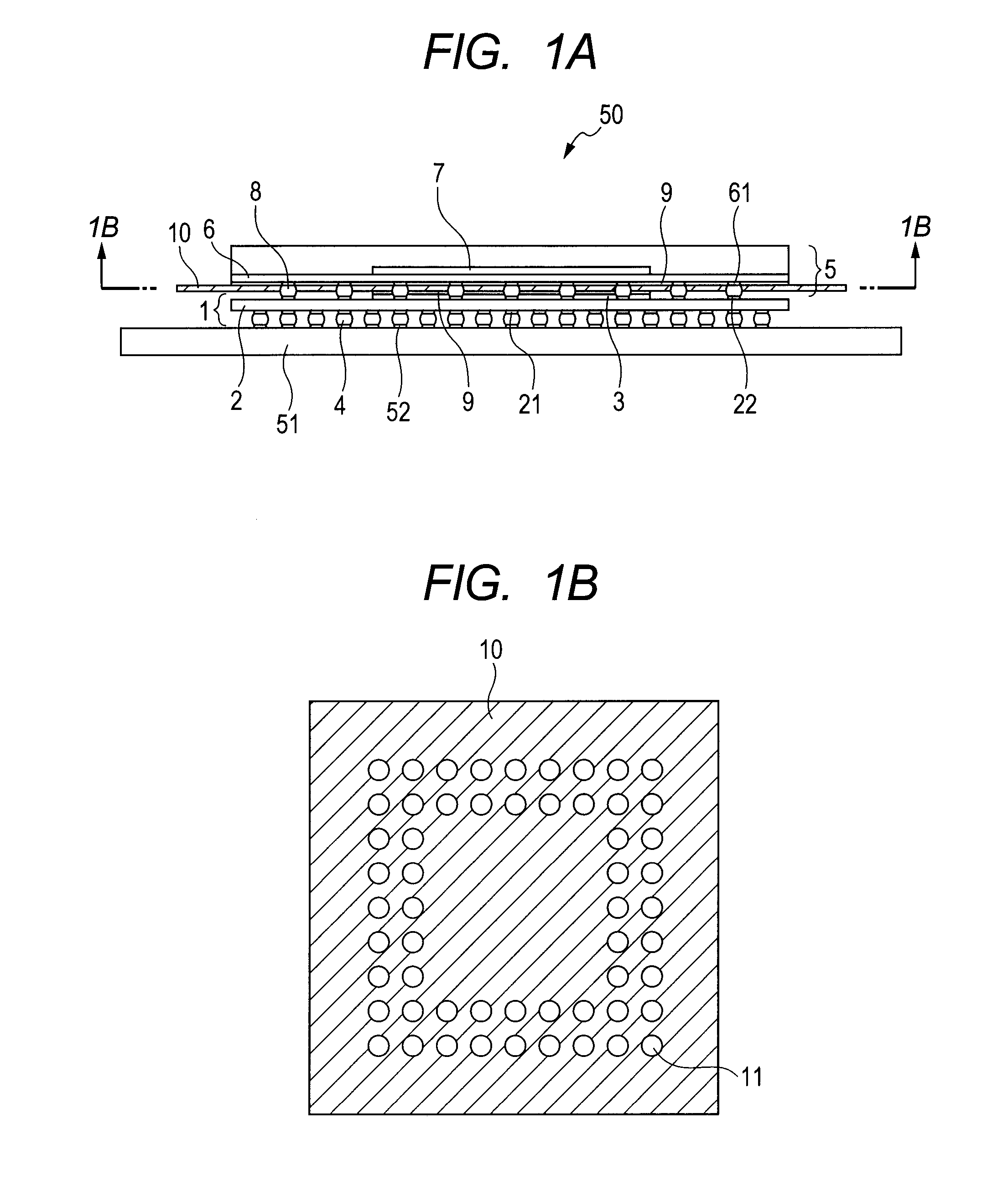
[0017]A first embodiment for carrying out the present invention is described in detail in the following with reference to the drawings. FIG. 1A is a sectional view of a stacked semiconductor device 50 according to the first embodiment of the present invention.

[0018]The stacked semiconductor device 50 includes multiple semiconductor packages, and in this embodiment, includes a first semiconductor package 1 and a second semiconductor package 5. The multiple semiconductor packages 1 and 5 are stacked via ball electrodes, and are three-dimensionally mounted on a motherboard 51. In other words, the stacked semiconductor device 50 in which the second semiconductor package 5 is stacked on the first semiconductor package 1 is mounted on the motherboard 51.

[0019]The first semiconductor package 1 includes a first wiring substrate 2 (also referred to as an interposer), a first semiconductor element 3 mounted on one surface (front surface) of the first wiring substrate 2, and multiple connectio...

example 1

[0052]In order to confirm the heat reduction effect of the stacked semiconductor device 50, thermal fluid analysis software (FLoTHERM V8.2 manufactured by Mentor Graphics) was used to perform a simulation. The shape and size of the simulation model of the stacked semiconductor device 50 were as follows.

[0053]The first wiring substrate 2 of the first semiconductor package 1 was a substrate in the shape of a square of 11.5 mm×11.5 mm. The thermal conductivity of the first wiring substrate 2 was 80 W / mK in a plane direction and was 0.5 W / mK in a thickness direction. The first semiconductor element 3 was in the shape of a square of 5 mm×5 mm and had a thickness of 0.05 mm. The thermal conductivity of the first semiconductor element 3 was 117.5 W / mK in the plane direction at 25° C. The number of the connection terminals 4 formed was 441, and the connection terminals 4 were in the shape of a square prism having a section which is a square of 0.34 mm×0.34 mm and having a height of 0.2 mm.

[...

second embodiment

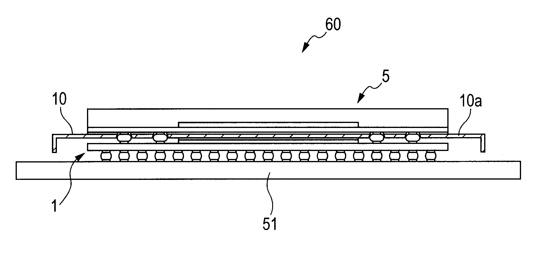
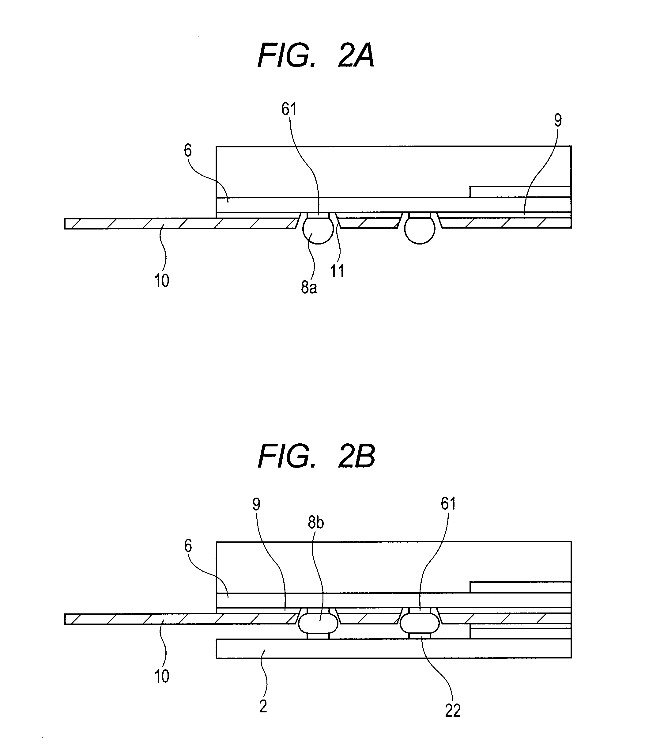
[0082]Next, a second embodiment for carrying out the present invention is described in detail with reference to the drawings. FIG. 5 is a sectional view of a stacked semiconductor device 60 according to the second embodiment of the present invention. Note that, like reference symbols are used to designate members similar to those in FIGS. 1A and 1B.

[0083]A heat dissipating member 10a of FIG. 5 is in such a shape that edges of the overhang are bent downward (toward the motherboard). Note that, the bent portion only needs to be provided at least at one edge of the overhang. With regard to the direction of the bending, it is more efficient to bend the overhang toward a lower atmospheric temperature side, and in this embodiment, the overhang is bent to the side of the first semiconductor package 1 which is directly mounted on the motherboard 51 and thus heat is more liable to be released therefrom.

[0084]With regard to the shape of the overhang, the heat dissipation effect thereof was co...


PUM


Abstract

Provided is a stacked semiconductor device (50) in which a semiconductor package (5) is stacked via connection terminals (8) on a semiconductor package (1), including a heat dissipating member (10) which is disposed between the semiconductor packages (1, 5), is brought into thermal contact with both of the packages (1, 5), and hangs over whole outer peripheral portions of the package (5). Such a structure causes heat generated from the package (5) to be released by heat dissipation into air above the package (5), heat dissipation into the air below the semiconductor package (5), heat transfer via the heat dissipating member (10) and a semiconductor element (3) to a first wiring substrate (2), heat transfer via the connection terminals (8) to the first wiring substrate (2), and heat dissipation via the heat dissipating member (10) into the air, thereby enhancing a temperature reduction effect of the semiconductor element.

Description

TECHNICAL FIELD[0001]The present invention relates to a stacked semiconductor device in which two or more semiconductor packages each having a semiconductor element mounted on a wiring substrate are stacked to be mounted three-dimensionally.BACKGROUND ART[0002]In recent years, various kinds of digital equipment such as digital cameras, digital camcorders, and cellular phones are becoming lighter and more compact, which requires a semiconductor package that may be mounted with a higher density.[0003]Now, as a mode which enables mounting with a high density, a stacked semiconductor device receives attention. A stacked semiconductor device is formed by further connecting a semiconductor package in which a semiconductor element is mounted on a wiring substrate to another semiconductor package. By three-dimensionally disposing semiconductor packages, the footprint may be reduced, which enables mounting with a high density.[0004]However, in a stacked semiconductor device, semiconductor el...

Claims


Application Information

Patent Timeline
IPC IPC(8): H01L23/34
CPCH01L23/36H01L25/105H01L23/34H01L24/16H01L24/48H01L2924/15331H01L2224/48227H01L2225/1023H01L2225/1058H01L2225/1094H01L2924/15311H01L2224/16225H01L2924/00014H01L2224/45099H01L2224/45015H01L2924/207
Inventor SUZUKI, TAKEHIRO
Owner CANON KK
Why Eureka
Try Eureka