Transporting machine

a technology of transporting arm and moving head, which is applied in the direction of gripping head, manufacturing tools, transportation and packaging, etc., can solve the problems of high electrical resistance on the back surface, difficult to increase the yield in the manufacturing process, and high static electricity dissipation property, so as to reduce vibration in the wafer, suppress the potential of the non-grounded state of the transporting arm, and the effect of high static electricity dissipation

Inactive Publication Date: 2009-12-15
ABLIC INC
View PDF13 Cites 2 Cited by
  • Summary
  • Abstract
  • Description
  • Claims
  • Application Information

AI Technical Summary

Benefits of technology

[0018]It is therefore an object of the present invention to reduce the vibration that occurs in the wafer during transportation.
[0025]According to the present invention, the transporting arm is coated with a substance having high static electricity dissipation property, whereby the static electricity, with which the transporting arm is charged, is discharged to the atmosphere more easily. Therefore, elevation of the potential of the transporting arm in the non-grounded state can be suppressed. As a result, reduction of the repulsive force acting between the transporting arm and the wafer enables reduction of vibration in the wafer caused by the effect of the static electricity.

Problems solved by technology

The silicon wafer, which has undergone the diffusion process and left as it is, has a problem such as high electrical resistance on the back surface due residual oxide thereof.
Even in a case of using the transporting machine as described above, difficulty in handling the silicon wafer ground to be thin to several hundreds μm in the back surface grinding process makes it difficult to increase yield in the manufacturing process.
When large vibration occurs during transportation due to the repulsive force, the wafer comes into contact with a partition portion and the like of the carrier and breaks, thereby reducing the yield in the manufacturing process.

Method used


Image

  • Transporting machine
  • Transporting machine
  • Transporting machine

Examples


Embodiment Construction

[0031]Hereinafter, a preferred embodiment of the present invention will be described in detail with reference to FIGS. 1 to 4.

(1) Outline of the Embodiment

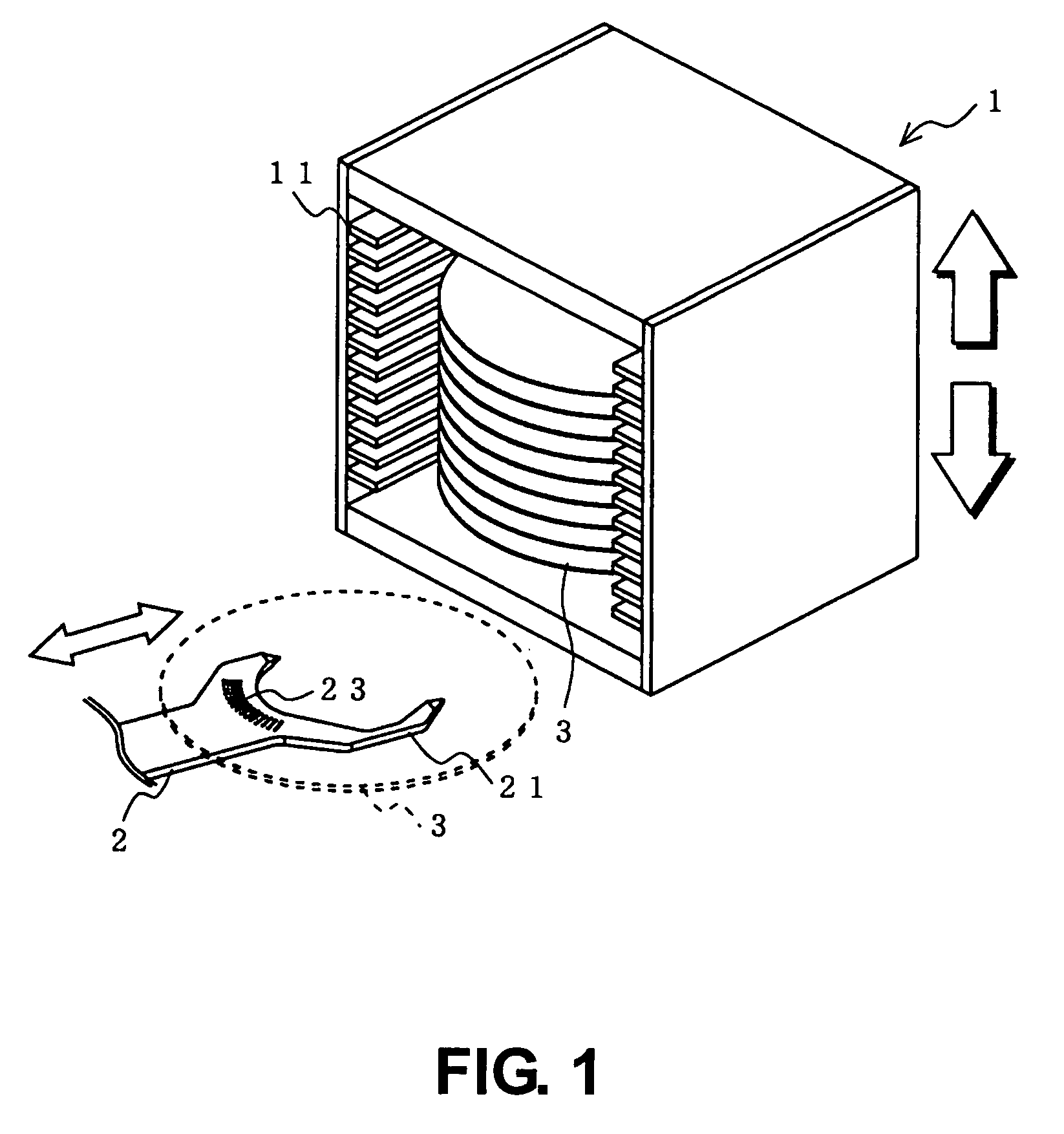
[0032]A description will be made on a wafer transporting system called a wafer loader for transporting thin silicon wafers, which are accommodated while being placed on partition plates (slits) of a wafer carrier, by allowing the silicon wafers to be sucked and fixed on a surface of the transporting arm one by one.

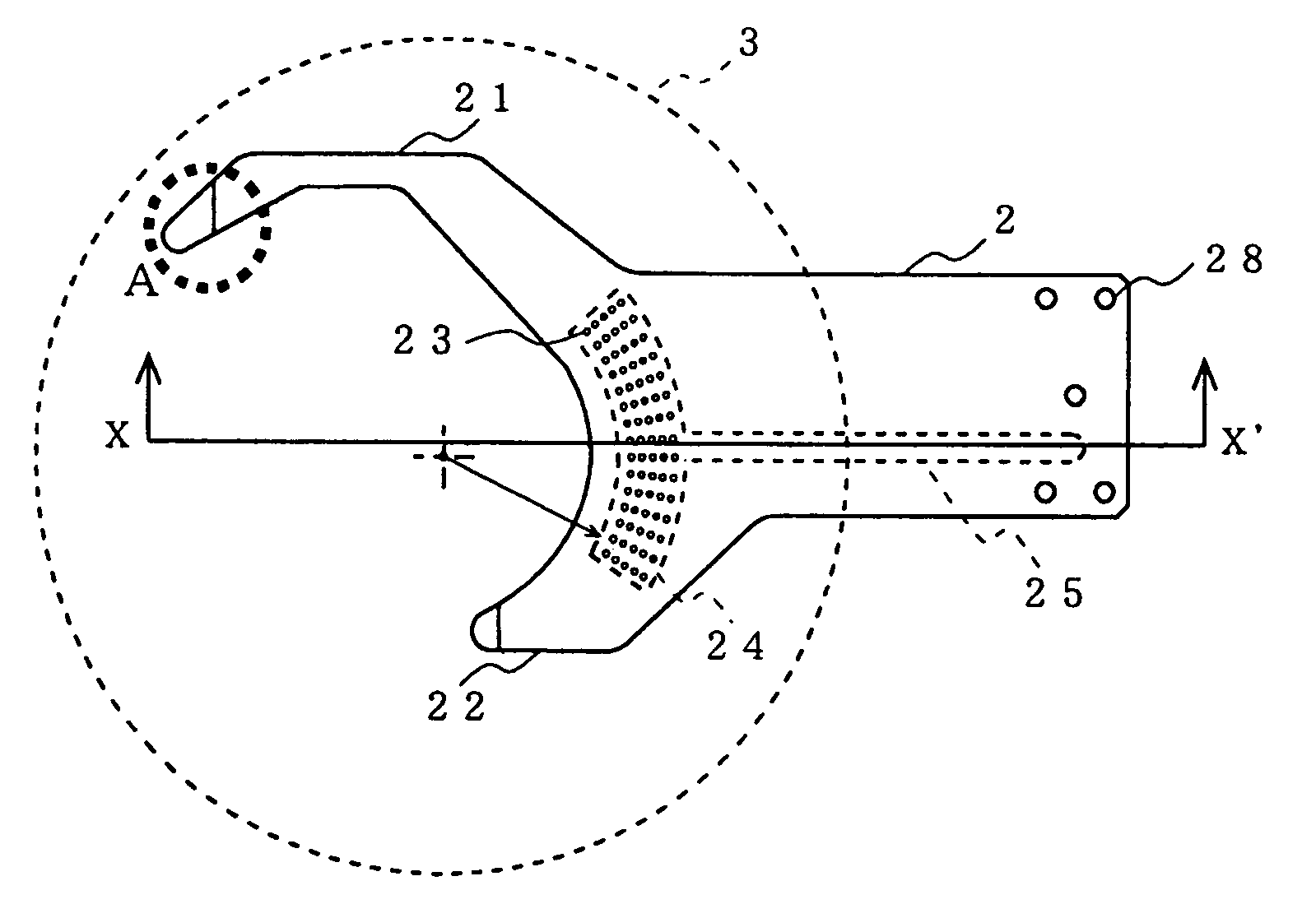
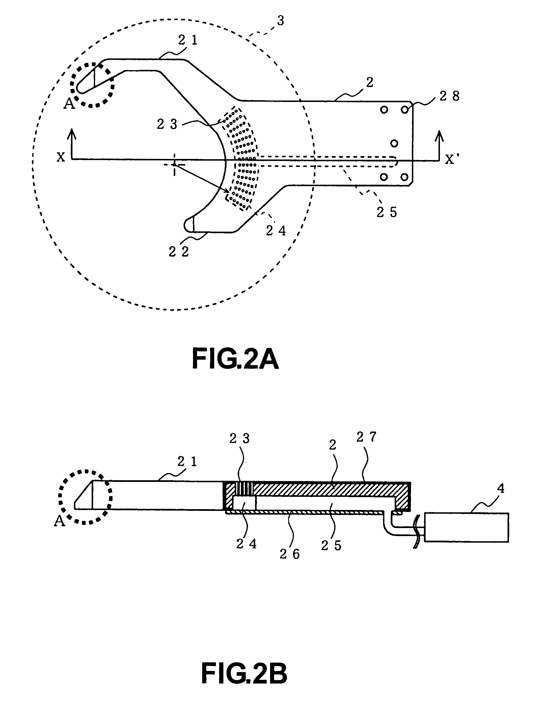
[0033]The transporting arm for transporting the silicon wafer has two protruding support sections of a fork shape (bifurcate) like a fork of a forklift.

[0034]Each of front ends of the support sections is formed such that the thickness thereof decreases toward a front portion (front end) thereof.

[0035]A surface of the transporting arm, on which the silicon wafer is to be placed, is provided with a plurality of suction holes formed in an inner portion of a fan-shaped region at equal intervals. By generating a vacuum in the...


PUM


Abstract

A transporting arm has two protruding support sections. Front ends of the support sections are formed such that a thickness of the support sections decreases toward the front ends of those. A surface of the transporting arm on which a wafer is placed is provided with a plurality of suction holes formed at equal intervals in a fan-shaped region. The wafer is fixed to the transporting arm through the suction holes. The wafer is charged with a large amount of static electricity. The transporting arm is charged with the static electricity. A surface of the transporting arm is coated with a conductive fluorinated graphite material. Therefore, an electrical discharge rate of the transporting arm into an atmosphere increases. Accordingly, elevation of a surface potential of the transporting arm in a floating state can be appropriately suppressed. Reduction of repulsive force due to the static electricity acting between the transporting arm and the wafer leads to reduction of vibration of the wafer.

Description

[0001]This application claims priority under 35 U.S.C. §119 to Japanese Patent Application No. JP2006-041907 filed Feb. 20, 2006, the entire content of which is hereby incorporated by reference.BACKGROUND OF THE INVENTION[0002]1. Field of the Invention[0003]The present invention relates to a transporting machine for transporting, for example, thin plate-like wafers.[0004]2. Description of the Related Art[0005]In a process of manufacturing an IC (semiconductor integrated circuit), after a wafer process of building an IC circuit onto a silicon wafer (including diffusion process, etching process, and photolithography process), an assembly process (including back surface grinding process, inspection process, and assembling process) is performed.[0006]In the inspection process in the assembly process, an inspection machine in which a microscope and the like are mounted is used to inspect basic function and characteristics as IC, thereby judging acceptability of a chip.[0007]The silicon w...

Claims


Application Information

Patent Timeline
Patent Type & Authority Patents(United States)
IPC IPC(8): B25J15/06
CPCH01L21/6838Y10T428/30Y10S414/141Y10S294/902H01L21/68
Inventor ASO, MAKOTO
Owner ABLIC INC
Why Eureka
Try Eureka