Semiconductor Device and Manufacturing Method thereof

Active Publication Date: 2013-04-04
INST OF MICROELECTRONICS CHINESE ACAD OF SCI
View PDF4 Cites 0 Cited by
  • Summary
  • Abstract
  • Description
  • Claims
  • Application Information

AI Technical Summary

Benefits of technology

[0027]The present invention provides a semiconductor device and its manufacturing method, wherein the NMOS device is covered by a layer of silicon nitride film having a high ultraviolet light absorption coefficient, said silicon nitride film can well absorb ultraviolet light when being subject to the stimulated laser surface anneal treatment so as to achieve a good dehydrogenization

Problems solved by technology

However, if the temperature is too high, the low temperature advantage and feature of PECVD will be

Method used


Image

  • Semiconductor Device and Manufacturing Method thereof
  • Semiconductor Device and Manufacturing Method thereof
  • Semiconductor Device and Manufacturing Method thereof

Examples


Example

[0032]The present invention will be described below by the preferred embodiments shown in the figures. However, it shall be understood that these descriptions are only exemplary, and are not intended to limit the scope of the invention. In addition, descriptions about the known structures and techniques are omitted below so as not to unnecessarily confusing the concept of the present invention.

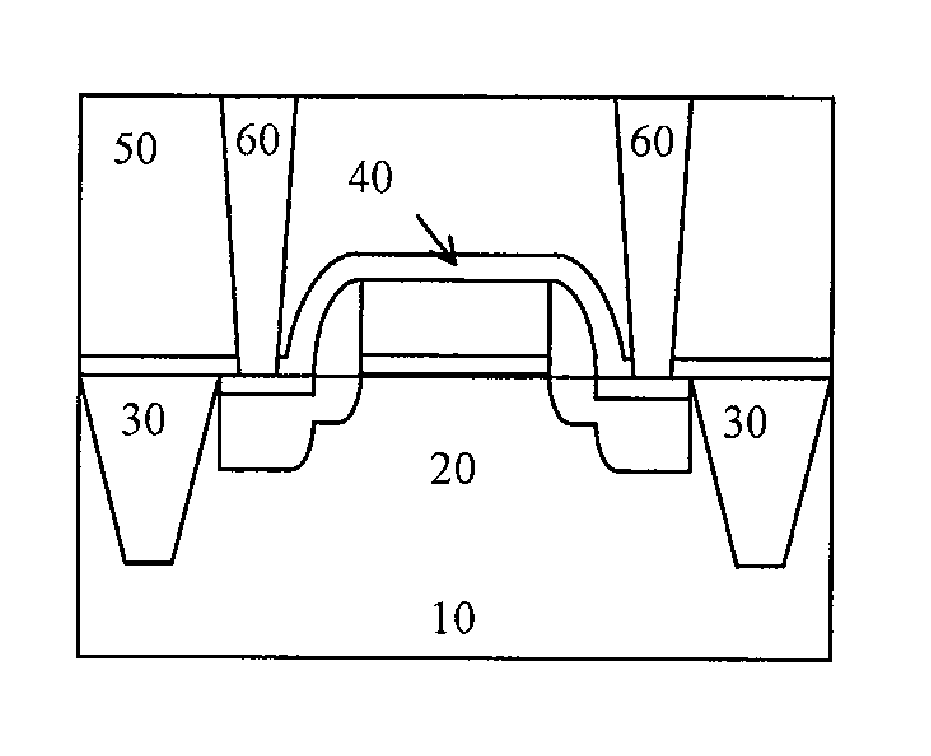
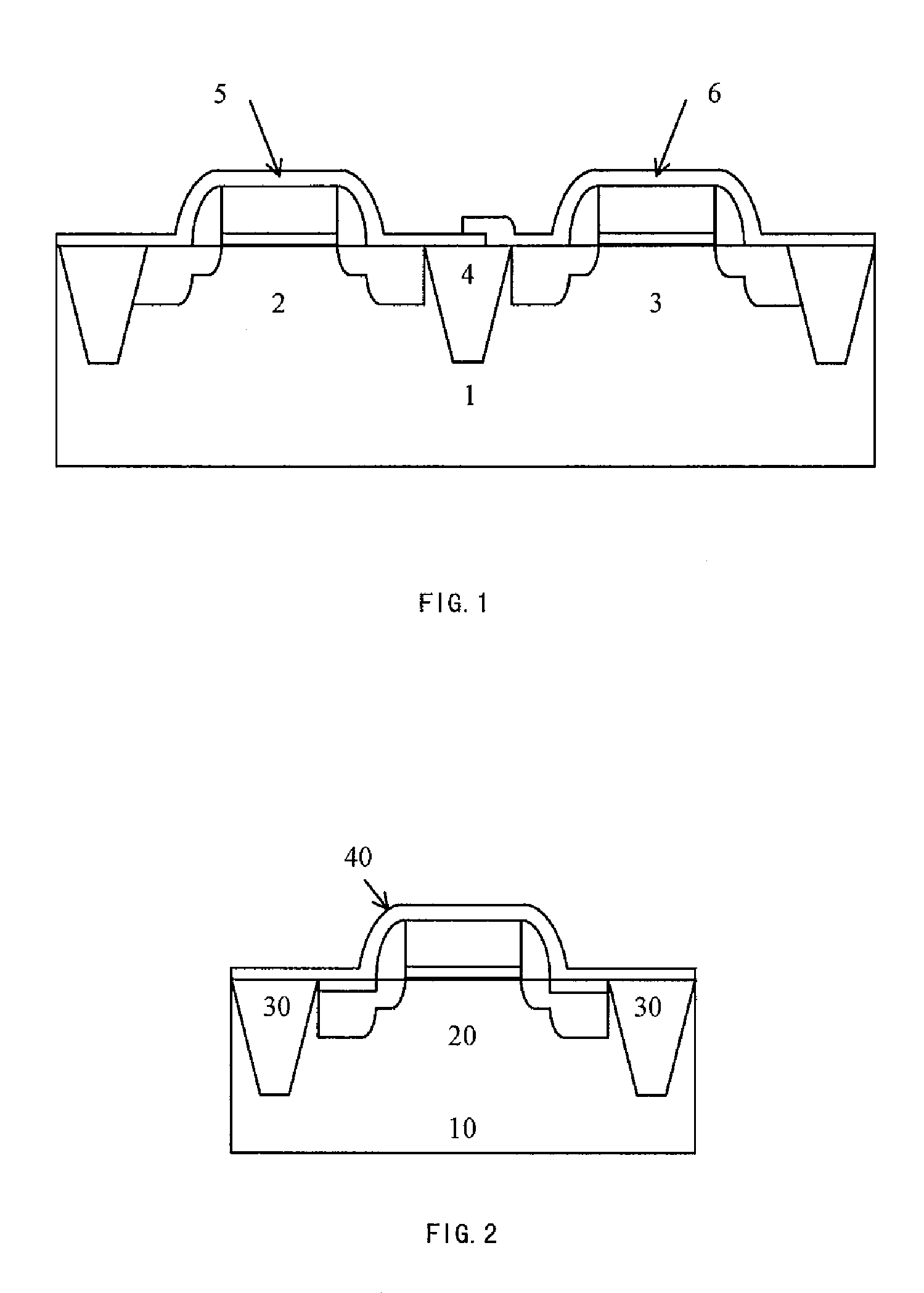
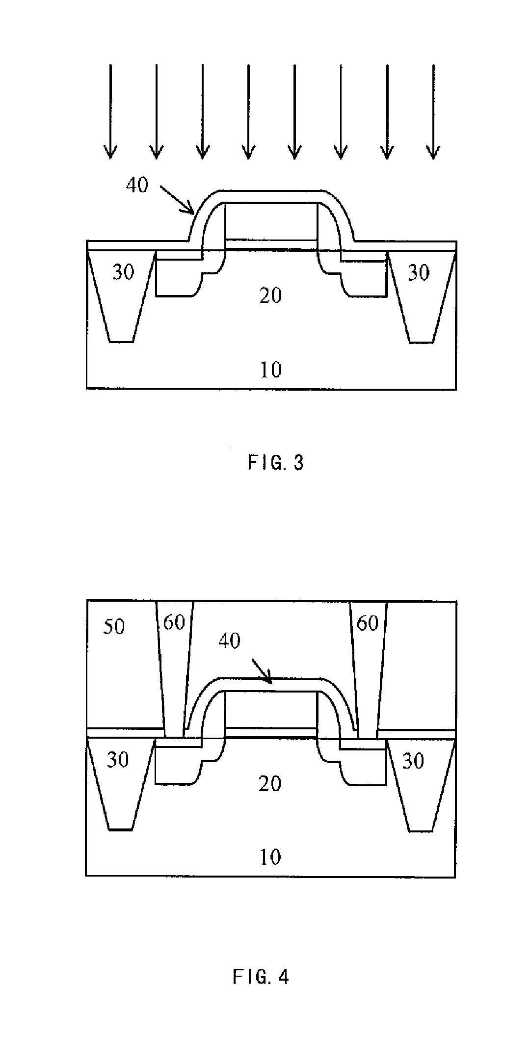
[0033]The present invention provides a semiconductor device manufacturing method, as shown in FIGS. 2-4.

[0034]First, a semiconductor substrate 10 is provided, on which an NMOS device 20 and an STI structure 30 are formed, as shown in FIG. 2.

[0035]Wherein, the semiconductor substrate 10 is a monocrystalline silicon substrate or SOI. The NMOS device 20 and the STI structure 30 can be formed by the known CMOS process in the art.

[0036]Then, a silicon nitride film having a high ultraviolet light absorption coefficient is deposited on the substrate 10 through a PECVD process. Then, lithography is pe...


PUM


Abstract

A semiconductor device and its manufacturing method, wherein the NMOS device is covered by a layer of silicon nitride film having a high ultraviolet light absorption coefficient through PECVD, said silicon nitride film can well absorb ultraviolet light when being subject to the stimulated laser surface anneal so as to achieve a good dehydrogenization effect, and after dehydrogenization, the silicon nitride film will have a high tensile stress; since the silicon nitride film has a high ultraviolet light absorption coefficient, there is no need to heat the substrate, thus avoiding the adverse influences to the device caused by heating the substrate to dehydrogenize, and maintaining the heat budget brought about by the PECVD process.

Description

CROSS REFERENCE[0001]This application is a National Stage Application of, and claims priority to, PCT Application No. PCT / CN2011 / 001964, filed on Nov. 25, 2011, entitled “Semiconductor Device and Manufacturing Method thereof”, which claims priority to Chinese Application No. 201110300828.5, filed on Sep. 29, 2011. Both the PCT application and the Chinese application are incorporated herein by reference in their entireties.FIELD OF THE INVENTION[0002]The present invention relates to a semiconductor device and the manufacturing method thereof, in particular to a structure and method for increasing thin film tensile stress of an MOS device.BACKGROUND OF THE INVENTION[0003]Strain Channel Engineering for increasing channel carrier mobility plays an important role in CMOS integrated circuits with a feature size smaller or equal to 90 nm. Uniaxial technologies for creating stress are integrated into the device technology. The NMOS and PMOS in a CMOS are covered by stress thin films, which ...

Claims


Application Information

Patent Timeline
IPC IPC(8): H01L29/02H01L21/31
CPCH01L21/268H01L29/6659H01L29/7833H01L21/3105H01L21/0217H01L21/823807H01L29/7843
Inventor YIN, HUAXIANGXU, QIUXIACHEN, DAPENG
Owner INST OF MICROELECTRONICS CHINESE ACAD OF SCI
Why Eureka
Try Eureka