
Far infrared imaging device and imaging method using same

a technology of infrared imaging and imaging method, which is applied in the field of infrared imaging, can solve the problems of unable to achieve compact and easy-to-use light sources emitted by light, limited use of electromagnetic waves, and delay in practical realization

Inactive Publication Date: 2013-04-11
HITACHI HIGH-TECH CORP
View PDF6 Cites 11 Cited by
  • Summary
  • Abstract
  • Description
  • Claims
  • Application Information

AI Technical Summary

Benefits of technology

The present invention provides a device and method to quickly image a specimen without using a high-power light source or causing damage or non-linear effects to the target.

Problems solved by technology

Conventionally, however, there are no compact and easy-to-use light sources emitting light in this range, and a detector therefor has to be cooled by liquid helium and so is hard to deal with, and therefore the usage of such electromagnetic waves have been only limited to research purposes.
In the case of a method based on the conventional point-measurement to move a specimen in x and y directions for imaging, however, it takes a few hours to acquire one image, which becomes a factor of delaying the practical realization.
When a measurement point is irradiated with high-power light for point measurement, however, the specimen may be damaged due to heat generated by absorption of optical energy, or a non-linear effect may occur due to the electric field intensity of the light, so that the measurement result may change.
However, such a method needs irradiation of a large area while maintaining the illuminance of illumination light, which requires a much higher-power light source.
When the output of a light source is insufficient, it takes a longer exposure time to acquire an image at one part, thus not leading much effect for speeding-up.

Method used


Image

  • Far infrared imaging device and imaging method using same
  • Far infrared imaging device and imaging method using same
  • Far infrared imaging device and imaging method using same

Examples


embodiments

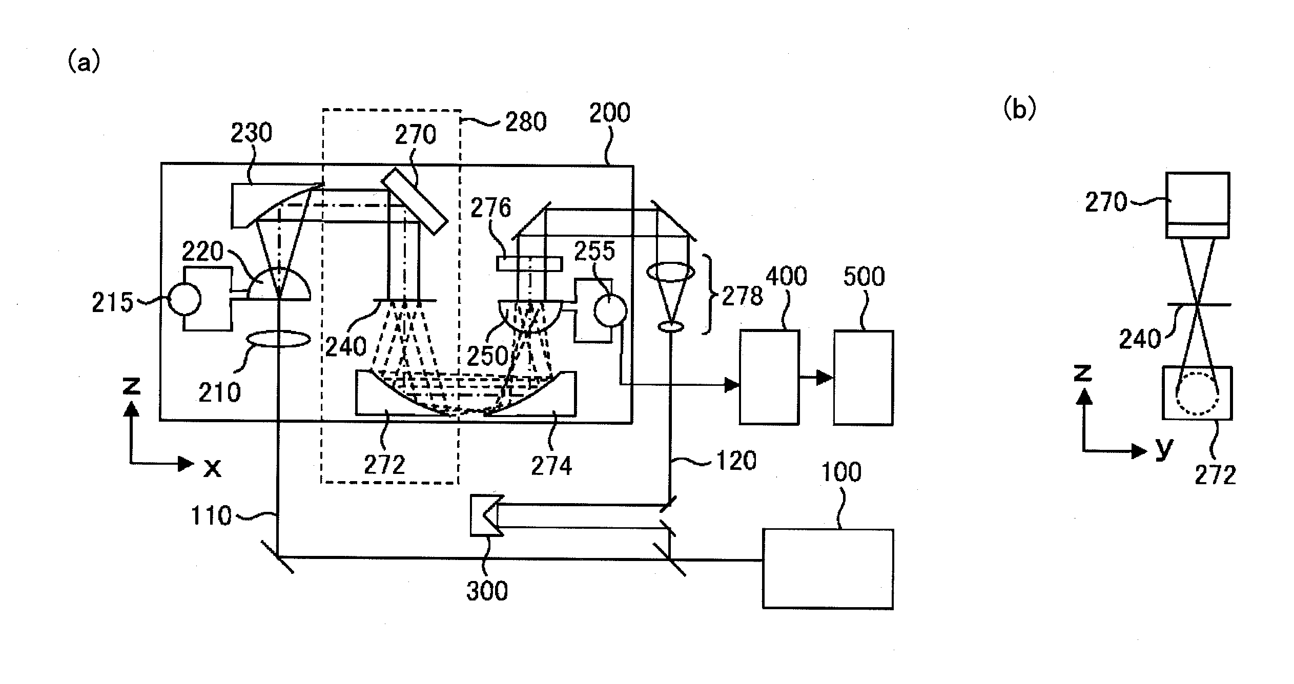
[0027]FIG. 1 schematically shows a configuration of a far infrared imaging device. The far infrared imaging device of FIG. 1(a) includes a femtosecond pulse light source 100, an imaging unit 200, an optical delay unit 300, a signal processing unit 400 and a control unit 500. Examples of the femtosecond pulse light source 100 include femtosecond titanium-sapphire lasers having the central wavelength from 780 nm to 800 nm, the pulse width from about 10 femtoseconds to 150 femtoseconds and the repetition frequency from about 50 megahertz to 100 megahertz as well as fiber lasers. Fiber lasers having 1.5 micrometer band also is available for this purpose. Femtosecond pulse light emitted from the femtosecond pulse light source 100 is divided by a beam splitter into pump light 110 used to generate far infrared light and probe light 120 used to detect far infrared light, which pass through an irradiation optical element 210 and a cylindrical lens 276 of the imaging unit 200, respectively, a...


PUM


Abstract

Provided are a far infrared imaging device that illuminates a specimen with far infrared light and detects an image of the specimen, which is a device capable of imaging a specimen speedily without using a high-power light source and without generating damage or a non-linear phenomenon in the specimen as a target to be imaged and a method using the same. A specimen is illuminated with the far infrared light in a line shape or in a shape of a plurality of points arranged in line on the specimen; and an image of the specimen is detected while moving the specimen in a direction perpendicular to the line illuminated by the far infrared light. The far infrared light is emitted by applying pulsed pump light from a femtosecond pulse light source to the far infrared light emission element.

Description

TECHNICAL FIELD[0001]The present invention relates to a far infrared imaging device to take images of a specimen using light in the far infrared region during testing such as analysis of the component distribution of chemical substances in the specimen or inspection of a dissimilar component or a foreign substance therein, and relates to an imaging method using the same.BACKGROUND ART[0002]Electromagnetic waves in the far infrared region from about 25 μm to 4 mm in wavelength are called terahertz waves as well. Since such electromagnetic waves have both properties of penetrability as radio waves and directionality as light and absorption spectra in this region have peaks specific to many substances, they are expected to be effective for identification of substances. Conventionally, however, there are no compact and easy-to-use light sources emitting light in this range, and a detector therefor has to be cooled by liquid helium and so is hard to deal with, and therefore the usage of ...

Claims


Application Information

Patent Timeline
IPC IPC(8): H04N5/33G01N21/3563G01N21/35G01N21/3586
CPCH04N5/33G01N21/3581H04N23/20
Inventor SHIMURA, KEINAKAI, NAOYA
Owner HITACHI HIGH-TECH CORP
Learn More