Optical read/write apparatus

a technology of optical read/write and optical head, which is applied in the direction of optical recording head, data recording, instruments, etc., can solve the problems of poor signal quality of read signal, difficult to increase the write rate, and difficulty in getting the verification operation done accurately, so as to minimize the influence of the write modulation waveform and perform the verification operation with stability

Active Publication Date: 2013-04-11
PANASONIC CORP
View PDF0 Cites 9 Cited by
  • Summary
  • Abstract
  • Description
  • Claims
  • Application Information

AI Technical Summary

Benefits of technology

[0027]An optical read / write apparatus as another embodiment of the present invention can write data on a track on an optical storage medium and read the data that has just been written on the track in parallel. The apparatus includes: a light source; an optical modulator configured to provide the light source with a write modulation signal that modulates the emission power of the light source according to the data to be written; a light-splitting element configured to split a light beam emitted from the light source into multiple light beams including a write beam and a read beam; an optical system configured to converge the write and read beams onto the same track on the optical storage medium so that while a write operation is being performed, the same location on the optical storage medium is scanned with the write beam before being scanned with the read beam; a photodetector including a light receiving element configured to detect the read beam reflected from the optical storage medium and output an electrical signal; a waveform predicting section configured to generate a predicted read waveform by performing processing that includes the step of delaying either the waveform of the write modulation signal or a waveform representing the write modulated component of the light beam that has been modulated with the write modulation signal; a comparing section configured to compare a waveform based on the output of the light receiving element to the predicted read waveform, thereby determining whether or not the data has been written successfully; and a delay detecting section configured to detect the time delay of a waveform representing the output signal of the light receiving element with respect to either the waveform of the write modulation signal or the waveform representing the write modulated component of the light beam that has been modulated with the write modulation signal, thereby controlling the amount of delay caused by the waveform predicting section based on the time delay detected.
[0036]An optical read / write apparatus as still another embodiment of the present invention can write data on a track on an optical storage medium that has multiple storage layers and read the data that has just been written on the track in parallel. The apparatus includes: a first light source configured to emit a write beam; a second light source configured emit a read beam; an optical modulator configured to modulate the emission power of the first light source according to the data to be written; an optical system configured to converge the write and read beams onto the same track on the optical storage medium so that while a write operation is being performed, the same location on the optical storage medium is scanned with the write beam before being scanned with the read beam; a photodetector including a light receiving element configured to detect the read beam reflected from the optical storage medium and configured to output an electrical signal; and an arithmetic unit configured to subtract a signal that is based on a signal obtained by detecting a part of the write beam that has been emitted from the first light source and then reflected from one of the storage layers other than a target storage layer to write data on, from the output signal of the light receiving element, thereby reducing modulated components produced by stray light that has come from the non-target storage layer from the output of the light receiving element.
[0039]An optical read / write apparatus as yet another embodiment of the present invention can write data on a track on an optical storage medium that has multiple storage layers and read the data that has just been written on the track in parallel. The apparatus includes: a first light source configured to emit a write beam; a second light source configured to emit a read beam; an optical modulator configured to provide the first light source with a write modulation signal that modulates the emission power of the first light source according to the data to be written; an optical system configured to converge the write and read beams onto the same track on the optical storage medium so that while a write operation is being performed, the same location on the optical storage medium is scanned with the write beam before being scanned with the read beam; a photodetector including a light receiving element configured to detect the read beam reflected from the optical storage medium and output an electrical signal; a waveform predicting section configured to generate a predicted read waveform by performing processing that includes the step of delaying either the waveform of the write modulation signal or a waveform representing the write modulated component of the light beam that has been modulated with the write modulation signal; a comparing section configured to compare a waveform based on the output of the light receiving element to the predicted read waveform, thereby determining whether or not the data has been written successfully; and a delay detecting section configured to detect the time delay of a waveform representing the output signal of the light receiving element with respect to either the waveform of the write modulation signal or the waveform representing the write modulated component of the light beam that has been modulated with the write modulation signal, thereby controlling the amount of delay caused by the waveform predicting section based on the time delay detected.
[0044]According to an embodiment of the present invention, it is possible to perform the verify operation with stability while minimizing the influence of a write modulation waveform on the output signal representing the reflected light that has left a read spot.

Problems solved by technology

Nevertheless, for a storage medium with a low degree of random accessibility such as the tape medium, it is difficult to increase the write rate as long as such a method of writing data and checking the data just written time-sequentially over and over again is adopted as in the known optical disc drive described above.
With any of these techniques, however, only a read signal of poor signal quality can be obtained and it is difficult to get the verify operation done accurately as will be described later.
Also, according to these known techniques, if any operating environment parameter such as the output power or the temperature changes, then the time delay between two signals to compare also changes, thus making it impossible to perform the comparison and correlation operations with good stability.
Furthermore, if the DRAW technique is applied to a storage medium with multiple information storage layers, the quality of the read signal will be debased due to the adverse influence of light that has been reflected from a storage layer other than the target one, from / on which data needs to be read or written.

Method used


Image

  • Optical read/write apparatus
  • Optical read/write apparatus
  • Optical read/write apparatus

Examples


embodiment 1

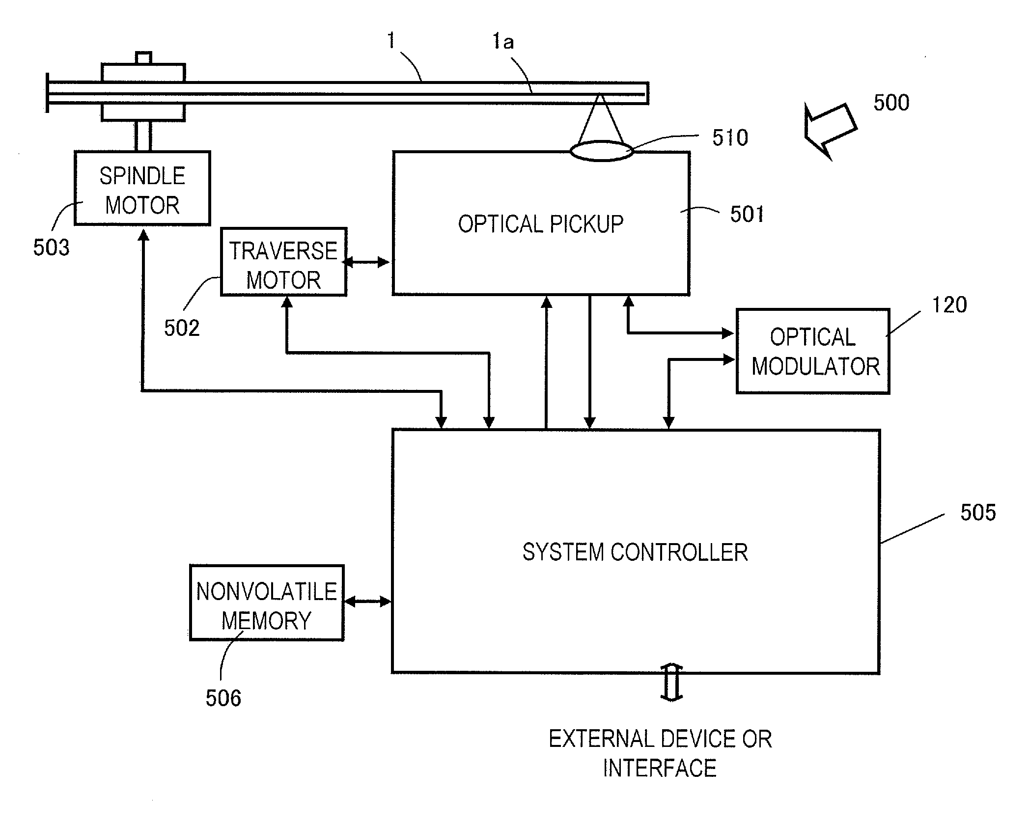
[0093]First of all, an optical read / write apparatus will be described as a first embodiment of the present invention. Before the specific configuration and operation of this embodiment are described, however, it will be described what problems with the related art should be overcome by the optical read / write apparatus of this embodiment.

[0094]According to the DRAW technique, in order to realize a simple and low cost optical pickup unit (OPU), structurally it will be beneficial to split the light emitted from a single light source into a read beam and a write beam. In particular, as for a read / write apparatus that performs a DRAW operation on a storage medium such as an optical tape using multiple optical pickups, a configuration for splitting the light emitted from a light source into a write beam and a read beam through a light-splitting element such as a diffraction grating or a hologram element will work fine and contribute to reducing its overall size and cost. If such a configu...

embodiment 2

[0130]Hereinafter, a second embodiment of an optical pickup and optical read / write apparatus according to the present invention will be described. The apparatus of this second embodiment has the same basic configuration as the first embodiment described above but uses a different signal processing configuration from that of the first embodiment. Thus, the following description of this second embodiment will be focused on the differences from the first embodiment and their common features will not be described all over again to avoid redundancies.

[0131]This embodiment provides an optical read / write apparatus and optical pickup that can perform comparison and correlation operations with good stability even if the time lag to be caused between a point in time when data is written with a write beam and a point in time when that data is read with a read beam has changed due to some variation in operating environment. First of all, the problem to be grappled with by this embodiment will b...

embodiment 3

[0164]Hereinafter, an optical pickup and optical read / write apparatus as a third embodiment of the present invention will be described. The optical pickup and optical read / write apparatus of this embodiment can overcome the problem that arises when a DRAW operation is performed on an optical storage medium with multiple storage layers. The optical read / write apparatus of this embodiment has basically the same overall configuration as what is shown in FIG. 1 but includes an optical pickup with a different arrangement and a system controller that performs different processing from their counterparts of the first embodiment described above. Thus, the following description of this third embodiment will be focused on those differences from the first embodiment and their common features will not be described all over again to avoid redundancies.

[0165]FIG. 20 illustrates the optical configuration of an optical pickup 901 for the optical read / write apparatus of this embodiment. As shown in ...


PUM

PropertyMeasurementUnit
wavelengthaaaaaaaaaa
widthsaaaaaaaaaa

Abstract

An optical read / write apparatus as an embodiment of the present invention includes: a light-splitting element configured to split a light beam emitted from a light source into multiple light beams including a write beam and a read beam; an optical system configured to converge the write and read beams onto the same track on an optical storage medium; a photodetector including a light receiving element configured to detect the read beam reflected from the optical storage medium and output an electrical signal; and a divider configured to generate a read signal by dividing the signal detected by the light receiving element by a signal that represents a write modulated component and that is obtained by detecting a part of the light beam emitted from the light source.

Description

BACKGROUND OF THE INVENTION[0001]1. Field of the Invention[0002]The present disclosure relates to an optical read / write apparatus that reads and writes information from / on an optical storage medium such as an optical tape, an optical disc or an optical card. More particularly, the present disclosure relates to an apparatus that carries out verification on data being written on an optical storage medium.[0003]2. Description of the Related Art[0004]Recently, the size of digital data to process has been rising steeply year by year as the resolutions of video data and still picture data have been tremendously increased and as increasing numbers of paper media have been converted into electronic ones. Meanwhile, so-called “crowd computing” technologies that allow people to use various kinds of applications and services via servers and storage systems on some network have become more and more popular nowadays. According to such crowd computing technologies, as a huge number of users save ...

Claims


Application Information

Patent Timeline
Patent Type & Authority Applications(United States)
IPC IPC(8): G11B7/135
CPCG11B7/1353G11B7/00458
Inventor KAYAMA, HIROSHIMOMOO, KAZUO
Owner PANASONIC CORP
Why Eureka
Try Eureka