Microfluidic chip

a microfluidic chip and microfluidic chip technology, applied in fluid controllers, laboratory glassware, nucleotide libraries, etc., can solve the problems of unsatisfactory detection precision and stability still have some drawbacks of conventional microfluidic chips, so as to achieve enhanced precision and stability

Inactive Publication Date: 2013-04-18
WAN CHIN FENG
View PDF4 Cites 13 Cited by
  • Summary
  • Abstract
  • Description
  • Claims
  • Application Information

AI Technical Summary

Benefits of technology

[0006]The present invention provides a microfluidic chip with enhanced precision and stability, so that applications of the microfluidic chip are more expansive.

Problems solved by technology

However, the conventional microfluidic chip still has some drawbacks.
Since the adhesion between the biological material and the photoresist material is insufficient, the detecting precision and stability of the conventional microfluidic chip are usually unsatisfied.

Method used


Image

  • Microfluidic chip
  • Microfluidic chip
  • Microfluidic chip

Examples


Embodiment Construction

[0012]The present invention will now be described more specifically with reference to the following embodiments. It is to be noted that the following descriptions of preferred embodiments of this invention are presented herein for purpose of illustration and description only. It is not intended to be exhaustive or to be limited to the precise form disclosed.

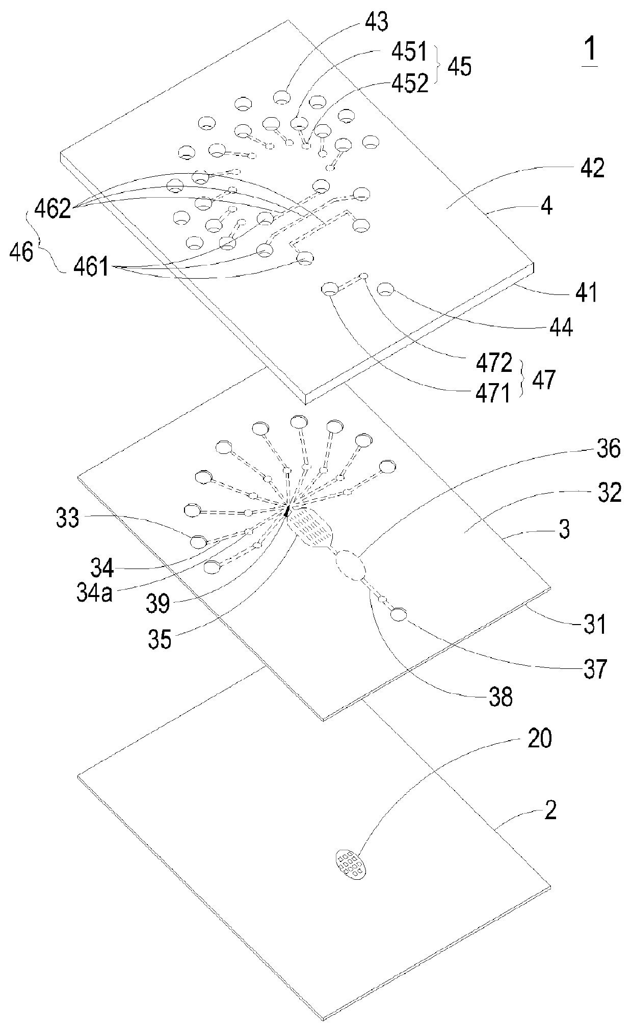
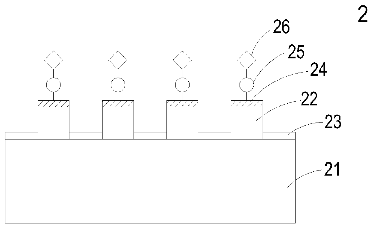
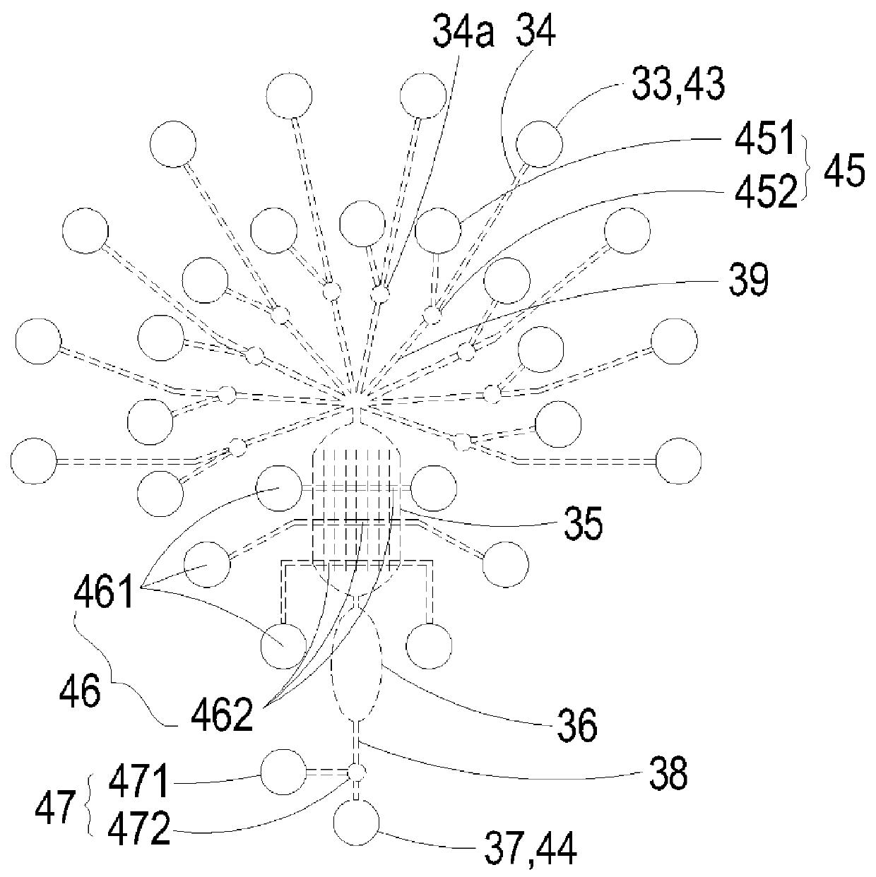
[0013]FIG. 1 is a schematic view illustrating the structure of a microfluidic chip according to an embodiment of the present invention. As shown in FIG. 1, the microfluidic chip 1 comprises a base layer 2, a fluid layer 3, and a gas regulating layer 4. The base layer 2 has a microarray detecting zone 20. The fluid layer 3 is disposed over the base layer 2 to cover the base layer 2. The fluid layer 3 has flow channels, wherein samples and detecting reagents may be introduced into or collected in the flow channels. The gas regulating layer 4 is disposed over the fluid layer 3 to cover the fluid layer 3. The gas regulating layer 4 i...


PUM

PropertyMeasurementUnit
diameteraaaaaaaaaa
thicknessaaaaaaaaaa
thicknessaaaaaaaaaa

Abstract

A microfluidic chip includes a base layer, a fluid layer, and a gas regulating layer. The base layer includes a microarray detecting zone. The microarray detecting zone includes a substrate, a photoresist pattern layer, a blocking layer, a bonding layer, at least one linker molecule, and a probe molecule. The bonding layer is covalently attached to the photoresist pattern layer. The at least one linker molecule is covalently bonded to the binding layer. The probe molecule is covalently bonded to the at least one linker molecule for specifically reacting with an under-test molecule. The fluid layer is disposed over the base layer, and includes plural flow channels for introducing or collecting detecting reagents. The gas regulating layer is disposed over the fluid layer for controlling open/close statuses of the flow channels, thereby controlling a flowing condition of a fluid in the fluid layer.

Description

FIELD OF THE INVENTION[0001]The present invention relates to a biochip, and more particularly to a microfluidic chip.BACKGROUND OF THE INVENTION[0002]A biochip is a miniaturized device that allows specific biochemical reactions between specified biological materials (e.g. nucleic acid or protein) and other under-test biological samples by employing a microelectromechanical systems (MEMS) technology. After the reaction signals are quantified by various sensors, the possible biochemical reactions can be realized. In other words, the miniaturized device fabricated by a microelectromechanical technology and a biological technology is referred as the biochip. For example, the biochip is a microfluidic chip or a lab-on-a-chip. The applications of the biochip cover the disease diagnosis, the gene probe, the pharmaceutical technology, the microelectronic technology, the semiconductor technology, the computer technology, and the like.[0003]Recently, due to the rapid development of the biomed...

Claims


Application Information

Patent Timeline
Patent Type & Authority Applications(United States)
IPC IPC(8): C40B40/06C40B40/10
CPCB01L3/502738B01L2300/0816B01L2300/0867B01J2219/00704B01L2400/0655B01J2219/00509B01J2219/00621B01L2400/0487
Inventor WAN, CHIN-FENG
Owner WAN CHIN FENG
Why Eureka
Try Eureka