Semiconductor device having metal gate and manufacturing method thereof

a technology of metal gate and semiconductor device, which is applied in the direction of semiconductor device, basic electric element, electrical apparatus, etc., can solve the problems of reducing the opening width of the gate trench, difficult to fill the gate trench with other materials, and the inability to form the filling metal layer in the gate trench as desired, so as to avoid seams and improve reliability

Inactive Publication Date: 2013-04-25
UNITED MICROELECTRONICS CORP
View PDF5 Cites 35 Cited by
  • Summary
  • Abstract
  • Description
  • Claims
  • Application Information

AI Technical Summary

Benefits of technology

[0009]According to the a semiconductor device having metal gate and manufacturing method thereof provided by the present invention, portions of the work function metal layers are removed from all the openings of the gate trenches after forming the second work function metal layer. Consequently, topmost portions of the first work function metal layer and of the second work function metal layer are all lower than the openings of the gate trenches, while the first work function metal layer and the second work function metal layer obtain a U shape. Therefore, the materials subsequently formed, such as the filling metal layer, are successfully formed in all gate trenches and thus seams are avoided. Accordingly, the semiconductor device having metal gate and manufacturing method provided by the present invention are prevented from the seam and the adverse impact rendered from the seams, and thus has the advantage of improved reliability.

Problems solved by technology

However, each layer formed in the gate trenches reduces an opening width of the gate trench by forming overhangs.
The overhang problem makes it difficult to fill the gate trench with the other material.
Serious overhang problem even results in a seam in the gate trench and makes the filling metal layer cannot be formed in the gate trench as desired.
Eventually, the electrical performance of the transistor device having the metal gate is deteriorated.
Furthermore, etching steps for removing the work function metal layer complementary to the required one damages the layers such as the inter layer dielectric (ILD) layer, and thus the metal materials may remain in the ILD layer and causes remnant metal defect.

Method used


Image

  • Semiconductor device having metal gate and manufacturing method thereof
  • Semiconductor device having metal gate and manufacturing method thereof
  • Semiconductor device having metal gate and manufacturing method thereof

Examples


Embodiment Construction

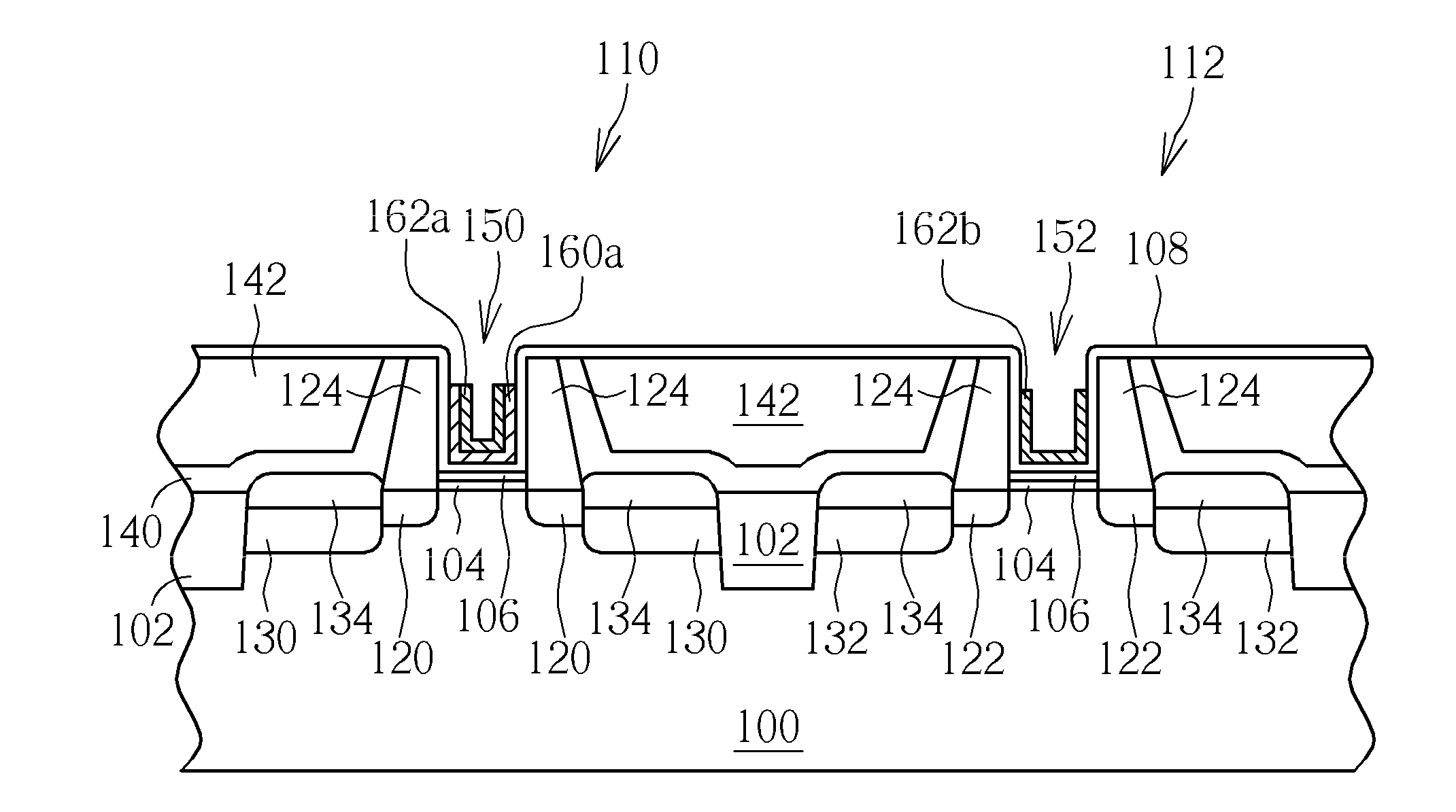
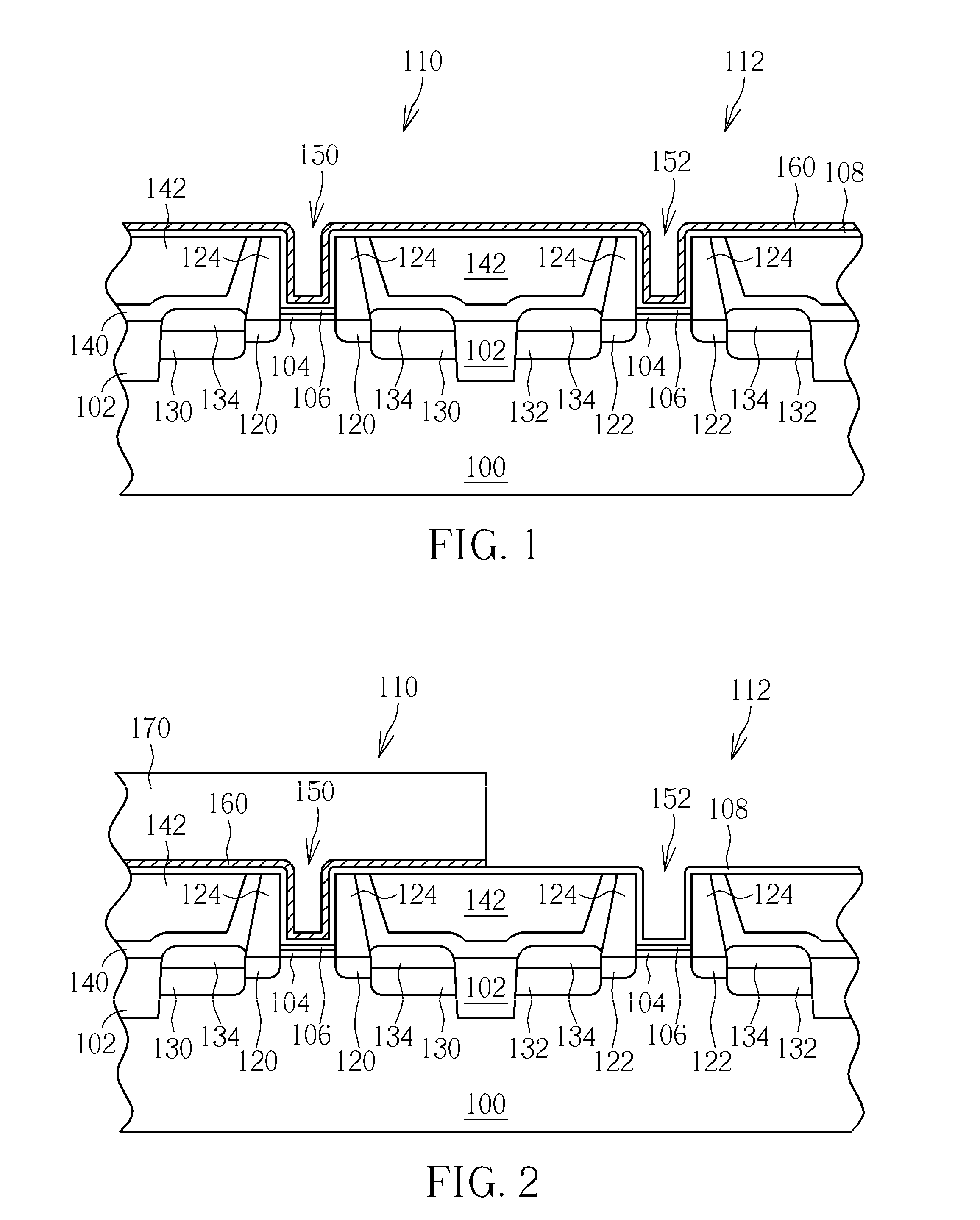
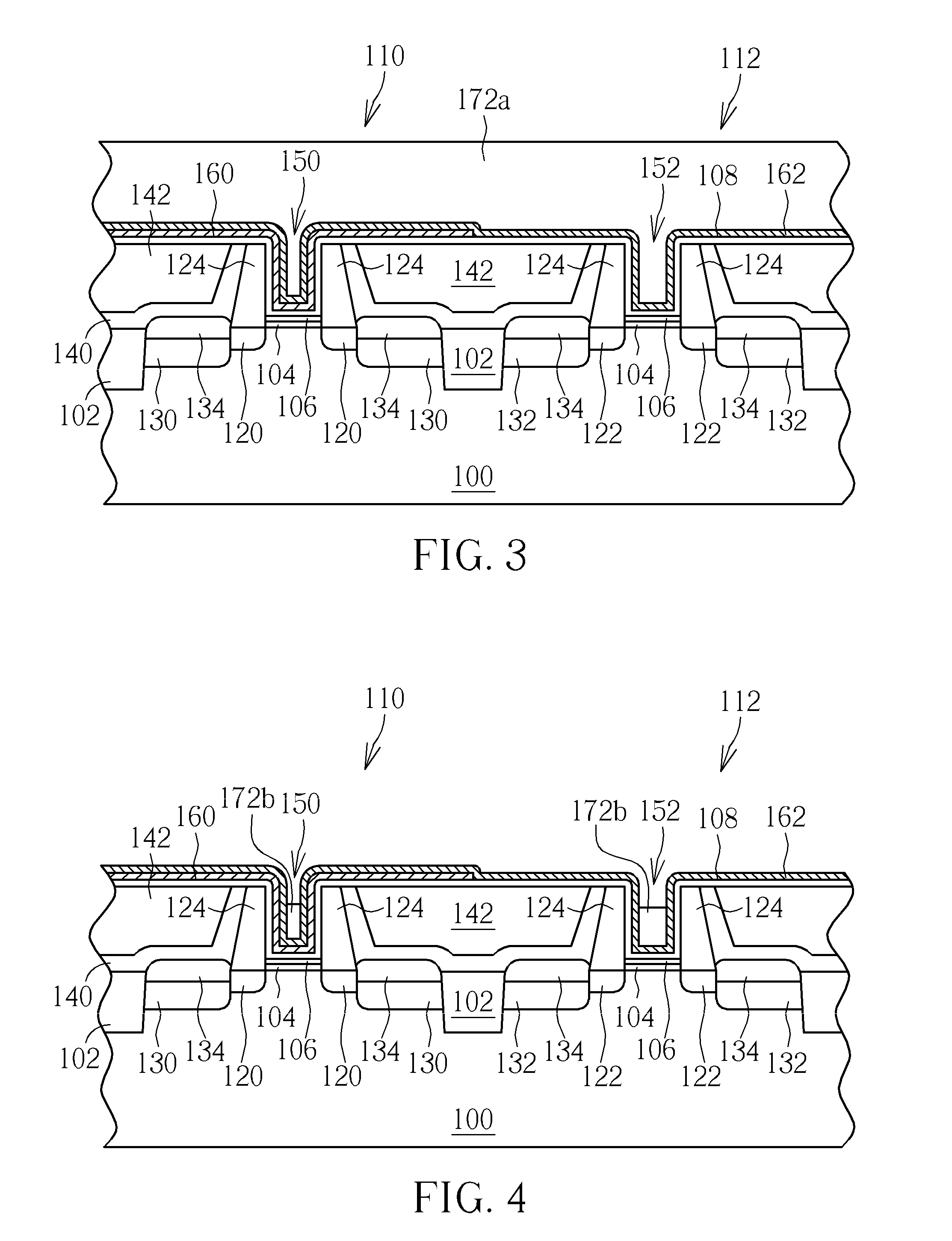
[0025]Please refer to FIGS. 1-6, which are drawings illustrating a manufacturing method for a semiconductor device having metal gate provided by a first preferred embodiment of the present invention. As shown in FIG. 1, the preferred embodiment first provides a substrate 100 such as silicon substrate, silicon-containing substrate, or silicon-on-insulator (SOI) substrate. The substrate 100 includes a first semiconductor device 110 and a second semiconductor device 112 formed thereon. A shallow trench isolation (STI) 102 is formed in the substrate 100 between the first semiconductor device 110 and the second semiconductor device 112 for providing electrical isolation. The first semiconductor device 110 includes a first conductivity type, the second semiconductor device 112 includes a second conductivity type, and the first conductivity type and the second conductivity type are complementary. In the preferred embodiment, the first conductivity type is p-type and the second conductivity...


PUM


Abstract

A manufacturing method of a semiconductor device having metal gate includes providing a substrate having a first semiconductor device and a second semiconductor device formed thereon, the first semiconductor device having a first gate trench and the second semiconductor device having a second gate trench, forming a first work function metal layer in the first gate trench, forming a second work function metal layer in the first gate trench and the second gate trench, forming a first patterned mask layer exposing portions of the second work function metal layer in the first gate trench and the second gate trench, and performing an etching process to remove the exposed second work function metal layer.

Description

BACKGROUND OF THE INVENTION[0001]1. Field of the Invention[0002]The invention relates to a semiconductor device having metal gate and manufacturing method thereof, and more particularly, to a semiconductor device having metal gate and manufacturing method integrated with the gate last process.[0003]2. Description of the Prior Art[0004]With a trend toward scaling down the size of the semiconductor device, work function metals are used to replace the conventional polysilicon gate to be the control electrode that competent to the high dielectric constant (high-K) gate dielectric layer. The conventional dual metal gate methods are categorized into the gate first process and the gate last process. Among the two main processes, the gate last process is able to avoid processes of high thermal budget and to provide wider material choices for the high-K gate dielectric layer and the metal gate, and thus gradually replaces the gate first process.[0005]In the conventional gate last process, a ...

Claims


Application Information

Patent Timeline
Patent Type & Authority Applications(United States)
IPC IPC(8): H01L29/78H01L21/762
CPCH01L21/28088H01L29/4966H01L29/513H01L29/517H01L21/823842H01L29/66545H01L29/66636H01L29/7848H01L29/518
Inventor TSENG, CHI-SHENGYANG, JIE-NINGHUANG, KUANG-HUNGWANG, YAO-CHANGLIAO, PO-JUIHSU, SHIH-CHIEH
Owner UNITED MICROELECTRONICS CORP
Why Eureka
Try Eureka