Solar cell and manufacturing method thereof

a solar cell and manufacturing method technology, applied in the field of solar cells, can solve the problems of increasing manufacturing costs, consuming a considerable amount of energy, and a relatively complicated whole process, and achieve the effects of reducing process costs, reducing furnace heat treatment process, and simplifying the process of manufacturing a solar cell

Inactive Publication Date: 2013-05-09
SAMSUNG SDI CO LTD
View PDF3 Cites 10 Cited by
  • Summary
  • Abstract
  • Description
  • Claims
  • Application Information

AI Technical Summary

Benefits of technology

[0029]According to an aspect of the exemplary embodiments, it is possible to simplify the process of manufacturing a solar sell since the process of forming the first semiconductor layer and the second semiconductor layer does not need to be repeatedly performed, and it is possible to reduce the process cost by reducing the furnace heat treatment process, which consumes a considerable amount of energy, to one time.
[0030]Further, according to an aspect of the exemplary embodiments, it is possible to relatively easily form the first semiconductor layer and prevent junction defects of the first semiconductor layer and the second semiconductor layer, by diffusing elements (e.g., uniformly diffusing group III elements).

Problems solved by technology

However, in the back contact solar cell, deposition, mask disposition, drive in diffusion (doping), and patterning processes need to be repeated twice so as to form a p-type semiconductor layer and an n-type semiconductor layer, and as a result, the whole process is relatively complicated.
In particular, an impurity doping process, which is a high temperature process of, for example, approximately 900° C. or more, is a process that consumes a considerable amount of energy.
Further, the impurity doping process needs to be repeated twice and, therefore, the manufacturing cost is increased.
Further, a junction may be formed in an undesired direction during the impurity doping process, and it is difficult to uniformly dope trivalent impurities at the time of forming the p-type semiconductor layer.

Method used


Image

  • Solar cell and manufacturing method thereof
  • Solar cell and manufacturing method thereof
  • Solar cell and manufacturing method thereof

Examples


Embodiment Construction

[0035]The present invention will be described more fully hereinafter with reference to the accompanying drawings, in which exemplary embodiments of the invention are shown. As those skilled in the art would realize, the described embodiments may be modified in various different ways, all without departing from the spirit or scope of the present invention. Further, it will be understood that when an element is referred to as being “on” another element, it can be directly on another element or intervening elements may be present therebetween.

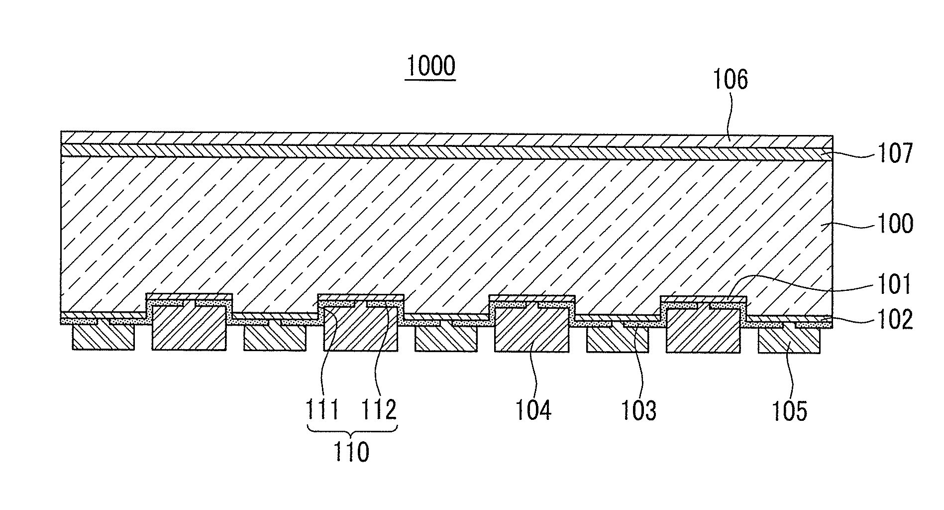
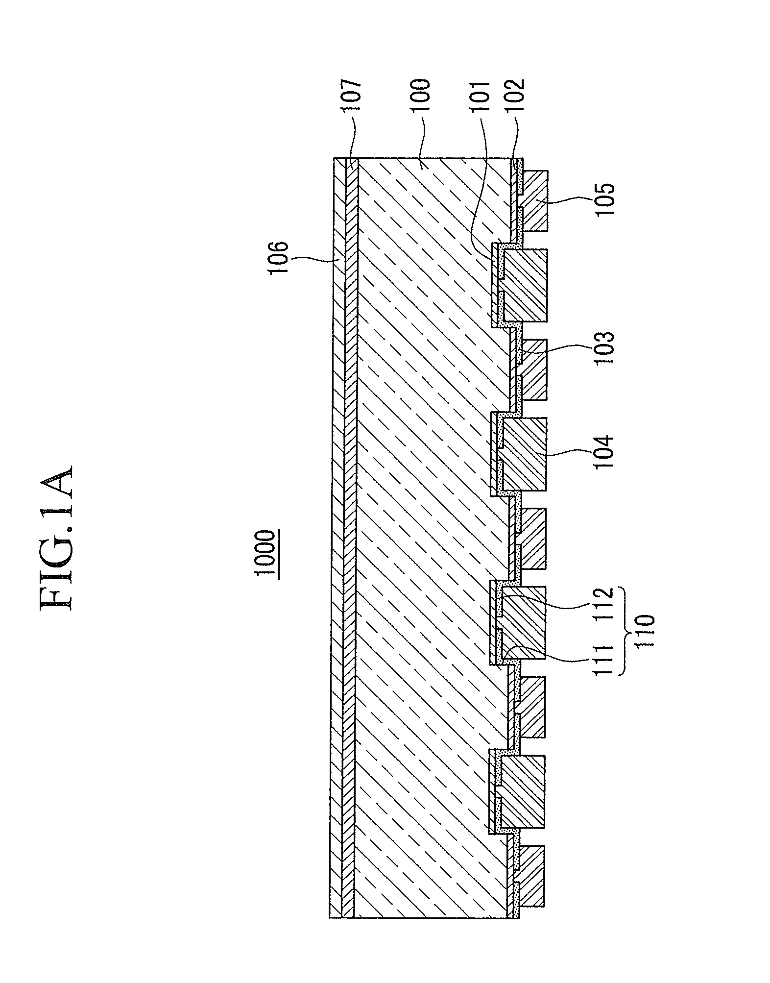
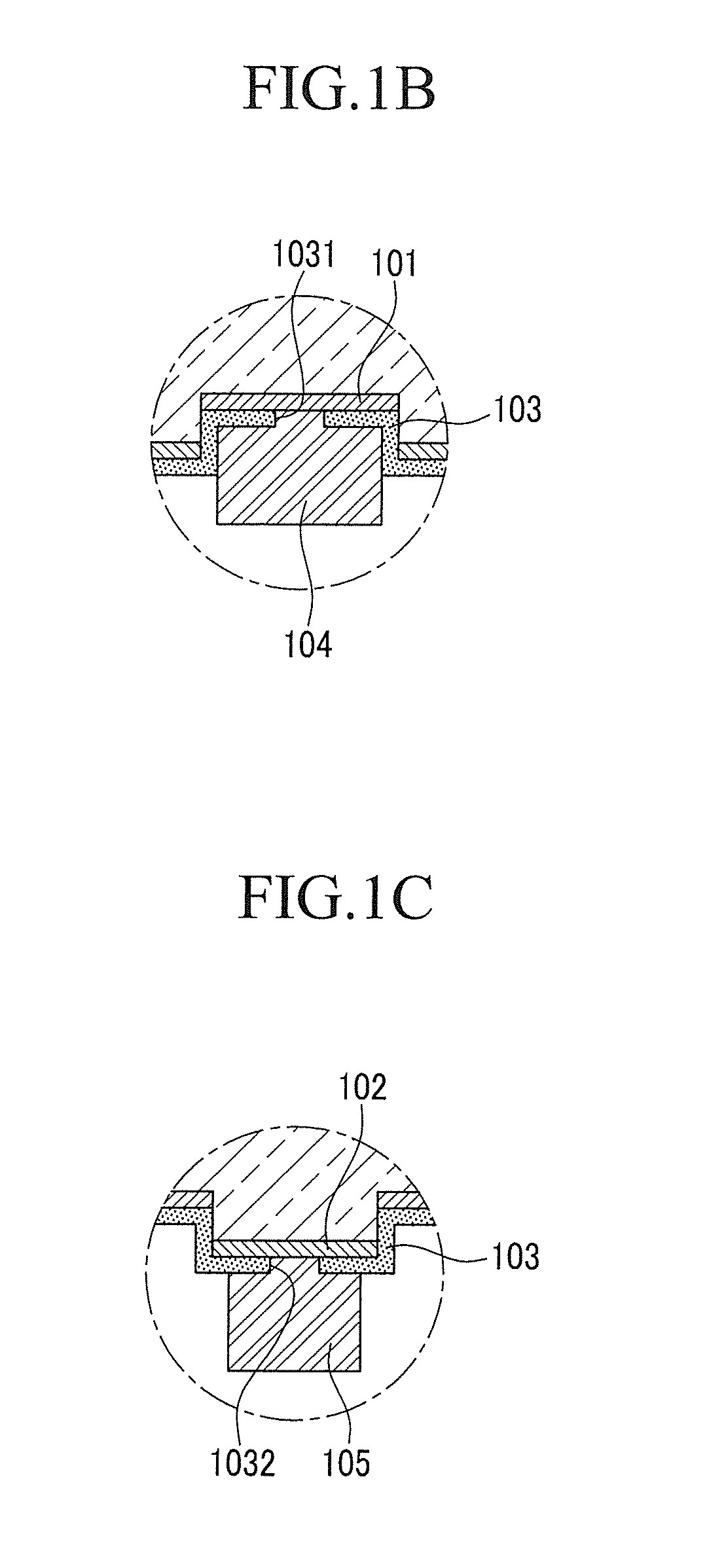
[0036]FIG. 1A is a schematic diagram of a solar cell according to a first exemplary embodiment, and FIGS. 1B and 1C are partially enlarged diagrams of the solar cell shown in FIG. 1A.

[0037]Referring to FIGS. 1A to 1C, a solar cell 1000 according to the first exemplary embodiment includes a semiconductor substrate 100, a first semiconductor layer 101 disposed on a back surface of the semiconductor substrate 100, a second semiconductor layer 102, a ...


PUM


Abstract

A solar cell including a first conductive type semiconductor substrate; a first conductive type first semiconductor layer on a back surface of the semiconductor substrate; a second conductive type second semiconductor layer on the back surface of the semiconductor substrate at a height different from the first semiconductor layer, the second semiconductor layer being separated from the first semiconductor layer; and a passivation layer on the back surface of the semiconductor substrate. The passivation layer covers at least a portion of the first semiconductor layer and at least a portion of the second semiconductor layer. The passivation layer includes impurities.

Description

CROSS-REFERENCE TO RELATED APPLICATION[0001]This application claims priority to and the benefit of Korean Patent Application No. 10-2011-0115942 filed in the Korean Intellectual Property Office on Nov. 8, 2011, the entire content of which is incorporated herein by reference.BACKGROUND[0002]1. Field[0003]The described technology relates generally to a solar cell, and more particularly, to a back contact solar cell and a manufacturing method thereof.[0004]2. Description of Related Art[0005]A back contact electrode solar cell has a structure in which all of a p-type semiconductor layer, a first electrode connected therewith, an n-type semiconductor layer, and a second electrode connected therewith, are disposed on a back surface of a solar cell that is an opposite surface of a light receiving surface. In the structure, a metal electrode is not positioned on the light receiving surface of the solar cell and thus, degradation in solar absorption due to the metal electrode may be prevente...

Claims


Application Information

Patent Timeline
Patent Type & Authority Applications(United States)
IPC IPC(8): H01L31/0352H01L31/18H01L31/065
CPCH01L31/02167H01L31/03529H01L31/0682H01L31/1804Y02E10/547Y02P70/50H01L31/0216H01L31/04H01L31/18
Inventor SEO, KYOUNG-JINLEE, CZANG-HOKIM, HYUN-JONGPARK, MINHONG, JUN-KIJEONG, BYONG-GOOK
Owner SAMSUNG SDI CO LTD
Why Eureka
Try Eureka