

Solar cell
a solar cell and semiconductor technology, applied in the field of semiconductor film and solar cell, can solve the problems of reducing the actual conversion efficiency of the solar cell and the band gap of the semiconductor, and achieve the effect of high energy conversion efficiency
- Summary
- Abstract
- Description
- Claims
- Application Information
AI Technical Summary
Benefits of technology
Problems solved by technology
Method used
Image

Examples
example
Preparation Example 1 of Semiconductor Film
[0067]CuxZnyInzSw film was formed on a soda-lime glass by the method of spraying thermal degradation. The specification is explained as in below.
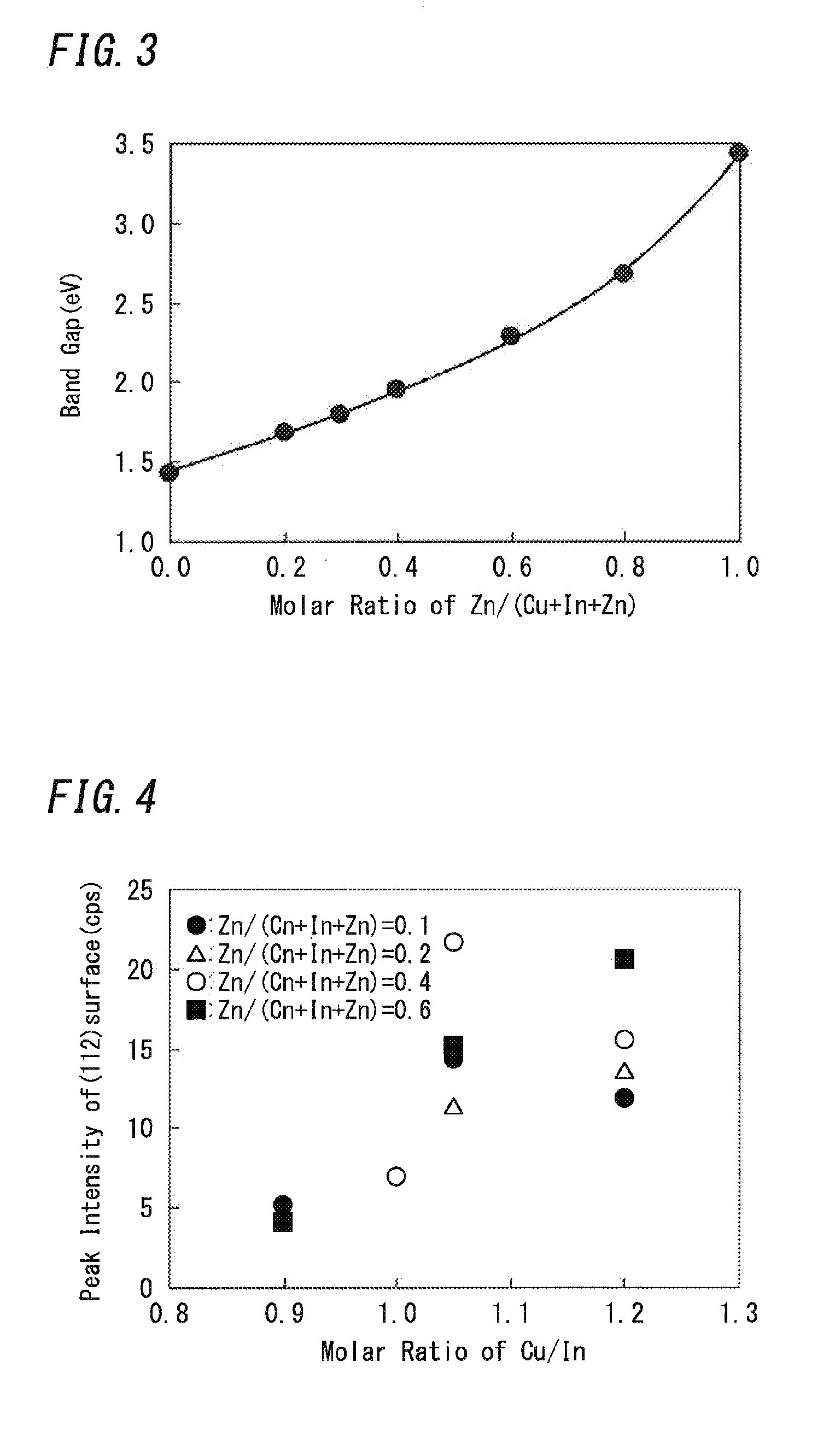
[0068]As a first step, multiple water solutions including CuCl2, InCl3, ZnCl2 and thiourea are prepared. In theses water solutions, the total molar concentration of CuCl2, InCl3 and ZnCl2 and the concentration of thiourea were adjusted to 4 mmmol / L and 10 mmol / L, respectively, and the molar ratio of Cu to In was adjusted to 1.05. The molar ratio of Zn / (Cu+In+Zn) of the solution was adjusted in the range of 0 to 1. When ZnCl2 was 0 mmol, the concentration of this solution was prepared to 2 mmol / L as well as the solution including CuCl2 and InCl3. In CuInS2 film which did not include Zn, when the molar ratio of Cu to In was 1 or more, the Cu—S phase was formed by excessive Cu and S. As a result, it was difficult to calculate the band gap of chalcopyrite phase consisting of CuInS2.
[0069]The solution w...
preparation example 1
of Solar Cell
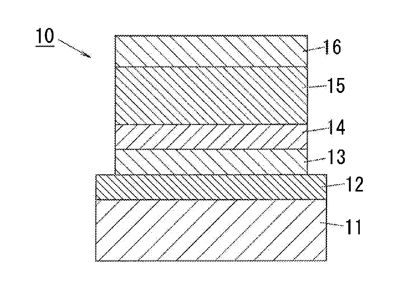
[0083]In this example, the base plate 11 formed of soda-lime glass was used. ITO was stacked on the base plate 11 by ultrasonic misting, and the transparent electrode 12 having 0.5 micro meters of thickness was formed on the base plate 11.
[0084]Next, the window layer 13 consisting of TiO2 was formed on the transparent electrode 12 by sputtering so as to have 0.1 micro meters of thickness. At this sputtering, the TiO2 sintered compact was used as target, Ar gas was filled within the instrument for sputtering, and the sputtering was carried out by the applied power of RF400W.
[0085]Next, the buffer layer 14 consisting of In2S3 was formed on the window layer 13 by the method of spraying thermal degradation so as to have the thickness of approximately 0.1 micro meters. At the spraying, the water solution including InCl3 of 2 mmol / L and thiourea of 6 mmol / L was sprayed on the window layer 13 heated until 300° C.
[0086]Next, the photo-absorbing layer 15 consisting of CuxZnyInzS...
preparation example 2
of Solar Cell
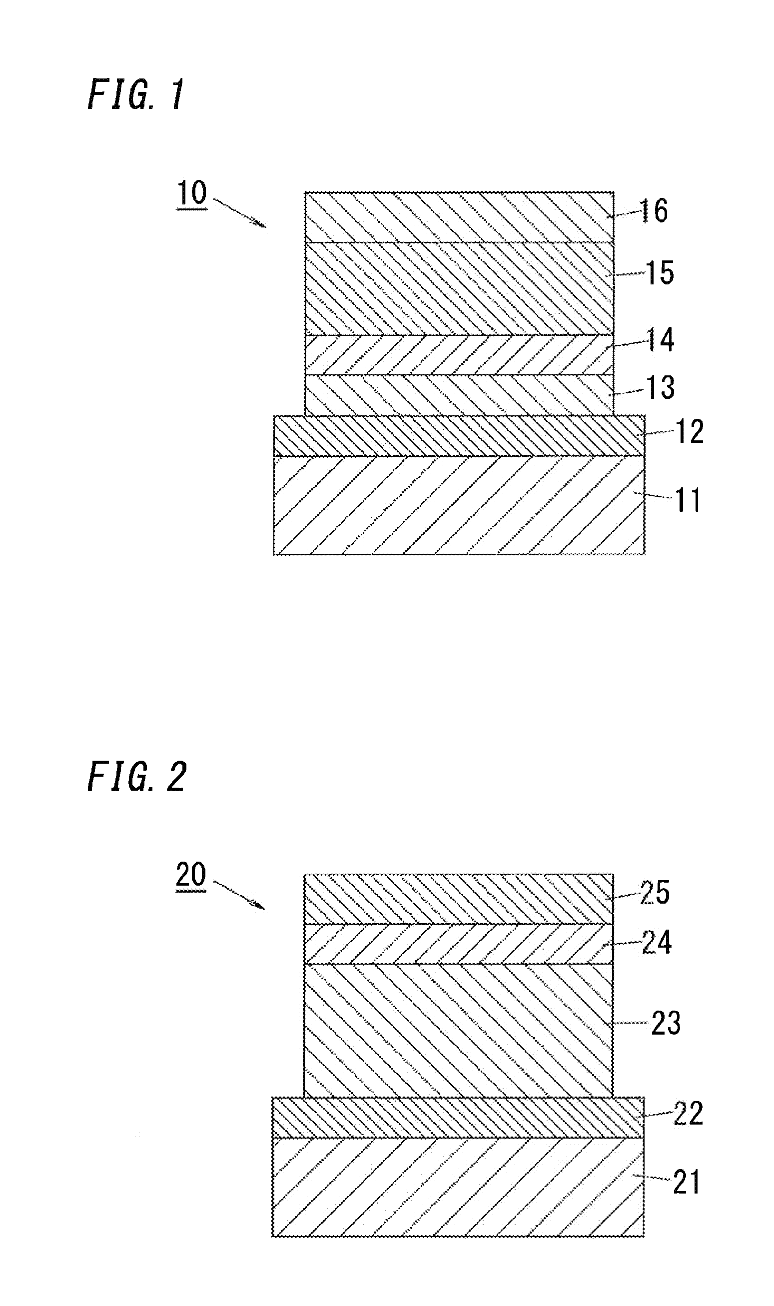
[0096]In this example, the base plate 21 formed of soda-lime glass was used. Mo was stacked on the base plate 21 by sputtering so as to become the first electrode 22 having the thickness of approximately 0.4 micro meters. At sputtering Mo, Mo was used as target, Ar gas was filled the atmosphere within the instrument for sputtering, and the sputtering was carried out by the applied power of DC 1 kW.
[0097]Next, the photo-absorbing layer 23 consisting of CuxZny(In, Ga)zSew film was formed on the first electrode 22 so as to have thickness of 2 micro meters. For forming the photo-absorbing layer 23, the deposition rate from evaporation source in each Cu, Zn, In, Ga, and Se was controlled, and the photo-absorbing layer 23 was stacked on the first electrode 22 in maximum base plate temperature of 550° C. The deposition rate is controlled so that the molar ratios of Zn / (Cu+In+Ga+Zn), Ga / (In+Ga), Cu / (In+Ga) within the CuxZny(In, Ga)zSew film are 0.25, 0.15 and 1.1, respectively....
PUM
 Abstract
Description
Claims
Application Information