

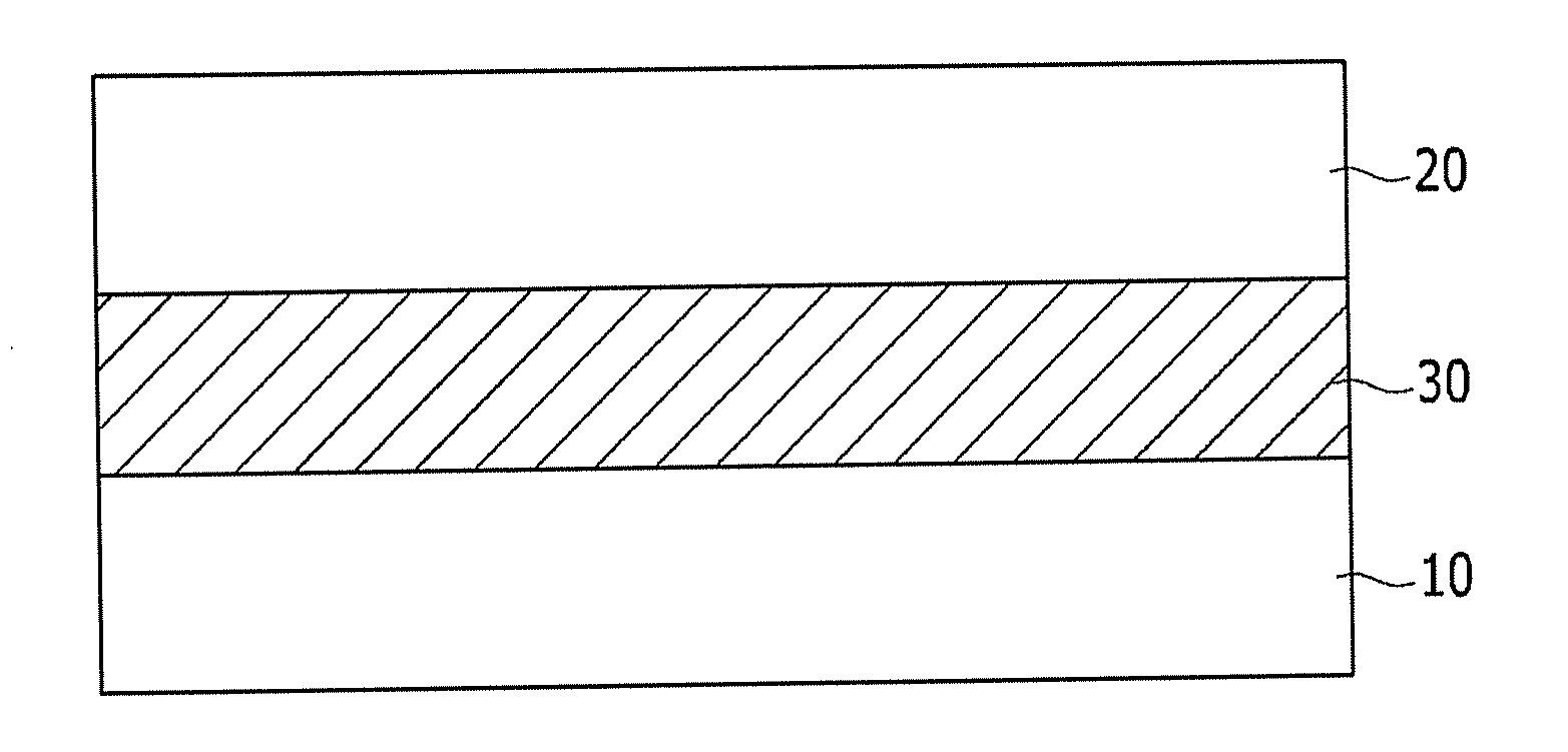
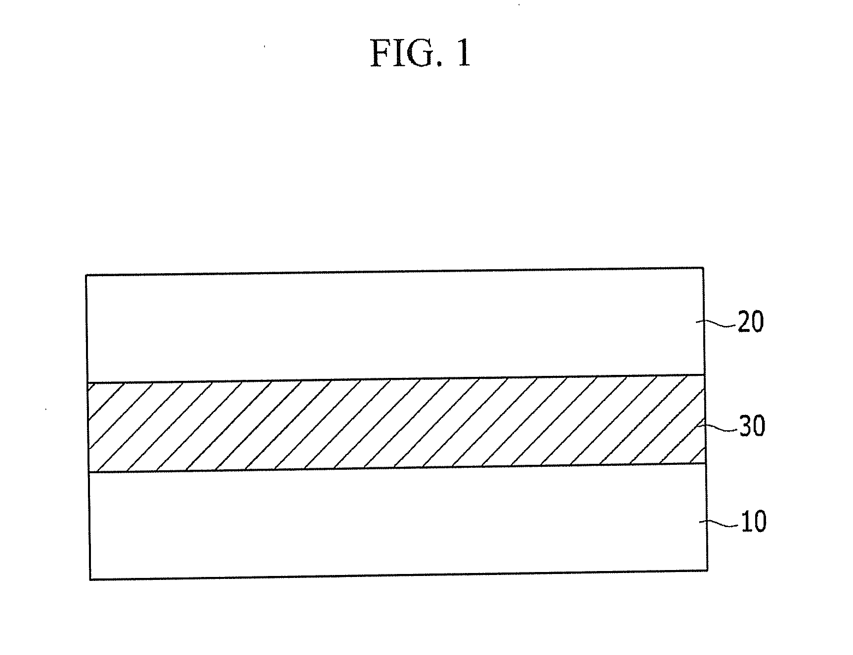
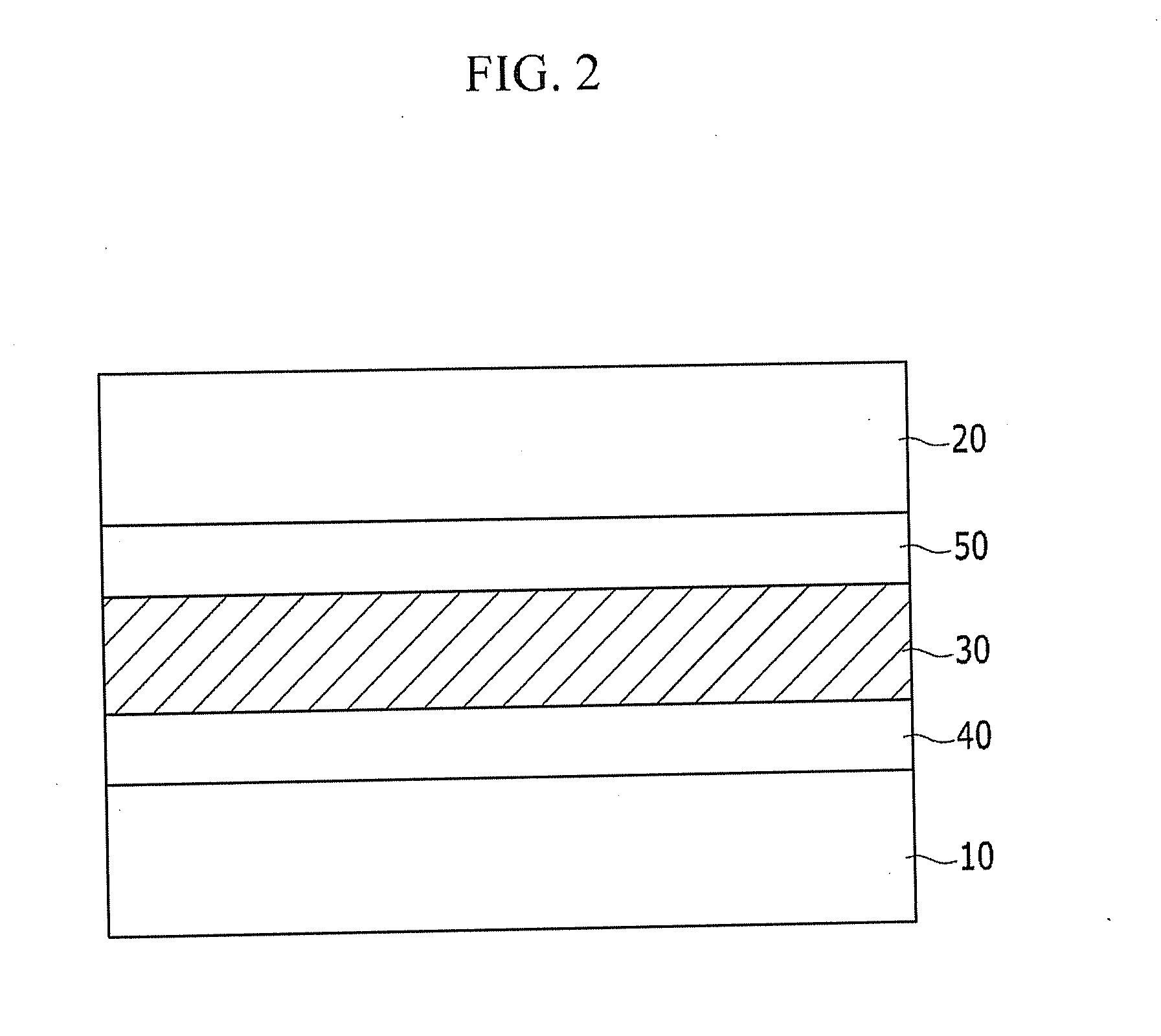
Organic photoelectronic device and image sensor
an image sensor and photoelectric device technology, applied in the direction of radiation control devices, non-metal conductors, applications, etc., can solve problems such as deterioration of sensitivity, and achieve the effect of improving efficiency
- Summary
- Abstract
- Description
- Claims
- Application Information
AI Technical Summary
Benefits of technology
Problems solved by technology
Method used
Image

Examples
example 1
[0091]ITO is sputtered on a glass substrate to form an approximately 100 nm thick anode, and a dimethylquinacridone compound represented by the above Chemical Formula 1a′ as a p-type semiconductor material is thermally deposited thereon to form a 30 nm-thick p-type layer. A dimethylquinacridone compound above Chemical Formula 1a′ as a p-type semiconductor material and a dicyanovinyl-terthiophene compound represented by the above Chemical Formula 2a as an n-type semiconductor material are co-deposited in a ratio of about 1:1 to form a 70 nm-thick active layer, and a dicyanovinyl-terthiophene compound represented the following Chemical Formula 2a as an n-type semiconductor material is thermally deposited thereon to form a 30 nm-thick n-type layer. Aluminum (Al) is sputtered on the n-type layer to form an 80 nm-thick cathode, finally fabricating an organic photoelectric device.
PUM
 Abstract
Description
Claims
Application Information