Circuits and methods for fault testing

a fault testing and circuit technology, applied in the field of electronic circuits, can solve problems such as signal delay faults, failures to detect faults, and failures to occur after the ic, and achieve the effect of significant ate and/or interface complexity and cos

Active Publication Date: 2013-05-09
ALLEGRO MICROSYSTEMS INC
View PDF5 Cites 10 Cited by
  • Summary
  • Abstract
  • Description
  • Claims
  • Application Information

AI Technical Summary

Benefits of technology

[0010]With this arrangement, accurate delay fault testing both at the wafer level and / or at the packaged IC level is achieved without requiring significant ATE and / or interface complexity and cost, by generating the high speed launch / capture test clock signal on the IC and in particular, by doing so in a way that does not require significant additional circuitry, using an oscillator that is already on the chip for other purposes.

Problems solved by technology

As digital semiconductor Integrated Circuit (IC) geometries become smaller and signal speeds become faster, fault testing becomes more challenging.
Various fault conditions such as marginal contacts, marginal vias, and marginal interconnects can cause signal delay faults.
While delay fault testing is easiest achieved and therefore predominantly preformed at the wafer level, before the semiconductor wafer is separated for individual IC packaging, certain faults may occur after the IC is packaged.
For example, the process of separating the semiconductor wafer and packaging the individual circuits can itself cause failures.
Device level testing is sometimes performed where applications require; however, such testing even more complex and costly DUT boards than wafer level testing.
However, stuck at fault testing may not be sufficient for certain critical applications.
However, there are difficulties in measuring such close edge spacing without adversely impacting the clock signal itself.
If the launch to capture pulse timing cannot be measured or measured accurately, then the potentiometer may be just adjusted until the DUT consistently passes a test, resulting in the test being run without accurate timing information.

Method used


Image

  • Circuits and methods for fault testing
  • Circuits and methods for fault testing
  • Circuits and methods for fault testing

Examples


Embodiment Construction

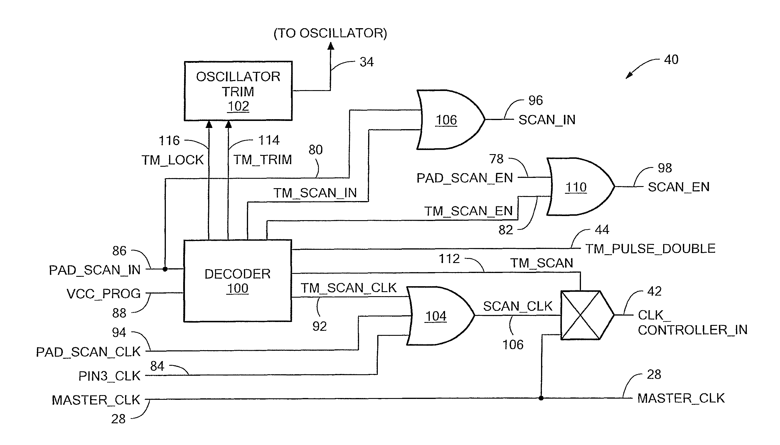
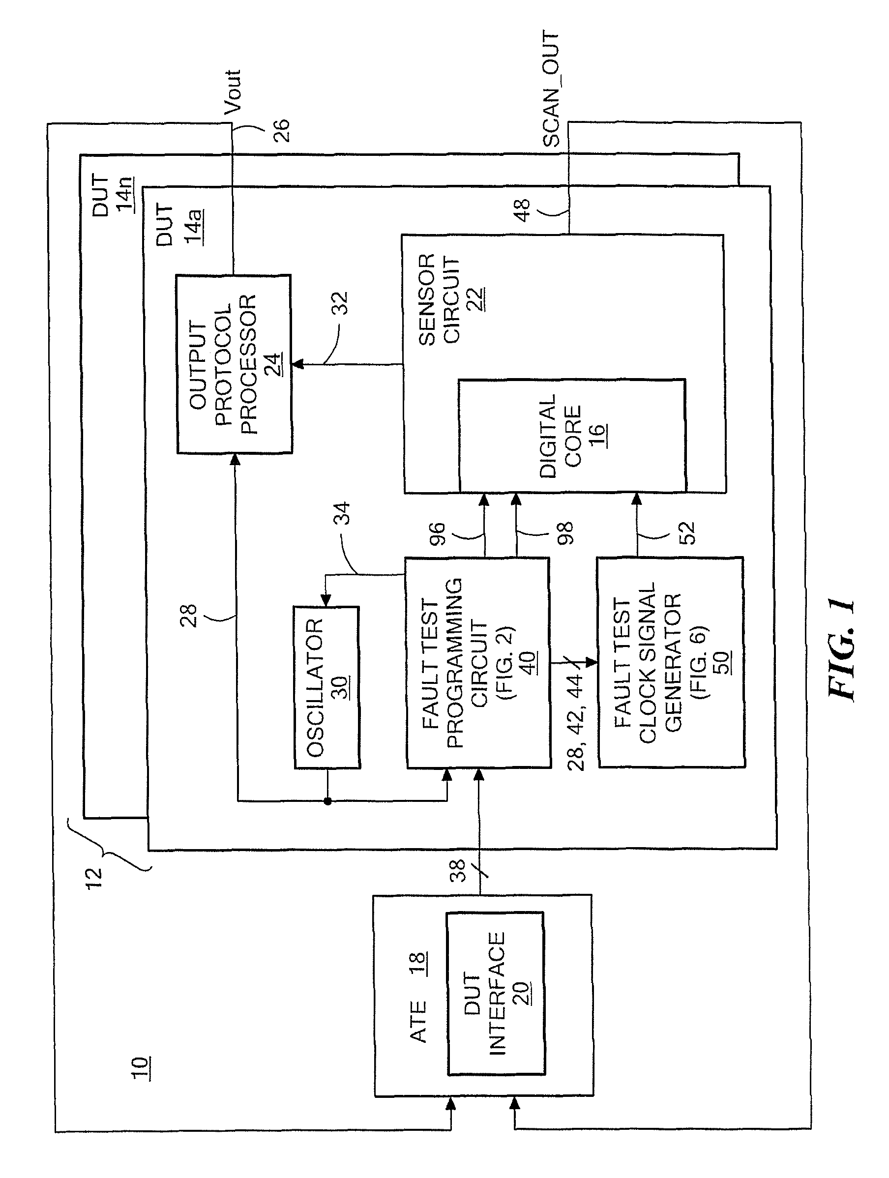
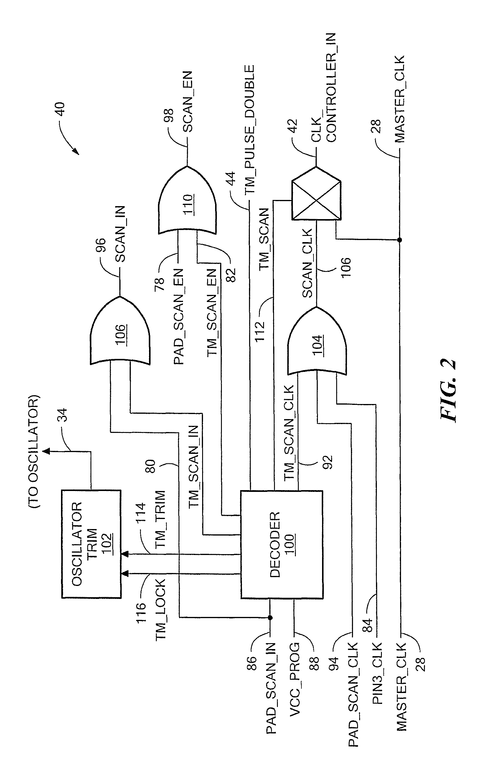
[0021]Referring to FIG. 1, a test system 10 for testing one or more electronic circuit devices, or Devices Under Test (DUTs) 14a-14n, is shown. The DUTs 14a-14n may take the form of semiconductor ICs or ASICs for a variety of applications, each including a digital core 16 for which fault testing is desired. Fault testing may be performed during a stage of manufacture when a semiconductor wafer 12 supports the DUTs 14a-14n (i.e., wafer level testing). An Automatic Test Equipment (ATE) unit 18 including a DUT interface 20 is coupled to the wafer 12 for this purpose. It may also be desirable to perform testing on each individual DUT 14a-14n after the wafer is diced and the DUTs are individually packaged in which case the ATE 18 (or an alternative less complex ATE) is coupled to the individual DUT 14a for example.

[0022]In the illustrative embodiment, each DUT 14a-14n (as shown and described in conjunction with illustrative DUT 14a which is referred to herein alternatively as sensor IC 1...


PUM


Abstract

An integrated circuit sensor includes circuitry and methods for generating a high speed delay fault test clock signal. A trimmable oscillator generates a master clock signal for use by an output protocol processor to provide the sensor output signal. A fault test clock signal generator is responsive to the master clock signal and to a test trigger signal for generating the test clock signal having a launch pulse and a capture pulse, each having edges substantially coincident with like edges of pulses of the master clock signal and a spacing between launch and capture pulses established by the trimmable master clock signal.

Description

CROSS REFERENCE TO RELATED APPLICATIONS[0001]Not Applicable.STATEMENT REGARDING FEDERALLY SPONSORED RESEARCH[0002]Not Applicable.FIELD OF THE INVENTION[0003]This invention relates generally to electronic circuits and, more particularly, to circuits and methods for delay fault testing.BACKGROUND OF THE INVENTION[0004]As digital semiconductor Integrated Circuit (IC) geometries become smaller and signal speeds become faster, fault testing becomes more challenging. Various fault conditions such as marginal contacts, marginal vias, and marginal interconnects can cause signal delay faults.[0005]Automatic Test Equipment (ATE) is used to generate test signals to exercise the digital IC and the resulting IC generated signals may be analyzed by the ATE and / or another external controller. An interface board, sometimes referred to as a Device Under Test (DUT) interface, is generally needed to adapt the ATE generated test signals to a particular IC. The ATE generated test signals generally inclu...

Claims


Application Information

Patent Timeline
Patent Type & Authority Applications(United States)
IPC IPC(8): G06F19/00
CPCG01R31/318552G01R31/318594
Inventor FORREST, GLENN A.COOK, AARONBRIERE, DANAFERNANDEZ, DEVONNAKAYAMA, NAOTA
Owner ALLEGRO MICROSYSTEMS INC
Why Eureka
Try Eureka