Integrated circuit with heat conducting structures for localized thermal control

a technology of integrated circuits and heat conducting structures, applied in the direction of semiconductor devices, semiconductor/solid-state device details, electrical apparatus, etc., can solve the problems of device reliability failure, high power consumption and heat generation, and more susceptible circuits to performance degradation, etc., to improve the thermal control of hot spots on the integrated circuit substrate, the effect of easy implementation

Active Publication Date: 2014-03-04
BELL SEMICON LLC
View PDF9 Cites 7 Cited by
  • Summary
  • Abstract
  • Description
  • Claims
  • Application Information

AI Technical Summary

Benefits of technology

[0014]Advantageously, the illustrative embodiments provide substantially improved thermal control of hot spots on an integrated circuit substrate. Moreover, the present invention in one or more of the illustrative embodiments can be readily implemented utilizing processing steps of a type commonly available in integrated circuit manufacturing, and thus without significant additional cost or complexity.

Problems solved by technology

With advances in semiconductor design and fabrication, the circuit density that can be implemented on a given integrated circuit die has steadily increased, leading to higher power consumption and heat generation.
Simultaneously, the scaling to finer geometries has exacerbated issues such as sub-threshold leakage current, making the circuits more susceptible to performance degradation due to temperature variations across the die.
Unfortunately, such a configuration may result in device reliability failures and other problems.
Heat dissipation with this configuration may simply be inadequate for higher power devices.
In addition, voids and poor coverage by the die attach layer, as well as inherent local high-power sources in the integrated circuit channel layer, may cause large temperature gradients across the integrated circuit die.
These gradients may cause regions of the die to be outside of the optimal operating temperature range, and may also cause mechanical stresses due to non-uniform thermal expansion.
However, these conventional approaches fail to provide an adequate solution to the problem of localized heat removal from high-power sources or other hot spots on an integrated circuit die.

Method used


Image

  • Integrated circuit with heat conducting structures for localized thermal control
  • Integrated circuit with heat conducting structures for localized thermal control
  • Integrated circuit with heat conducting structures for localized thermal control

Examples


Embodiment Construction

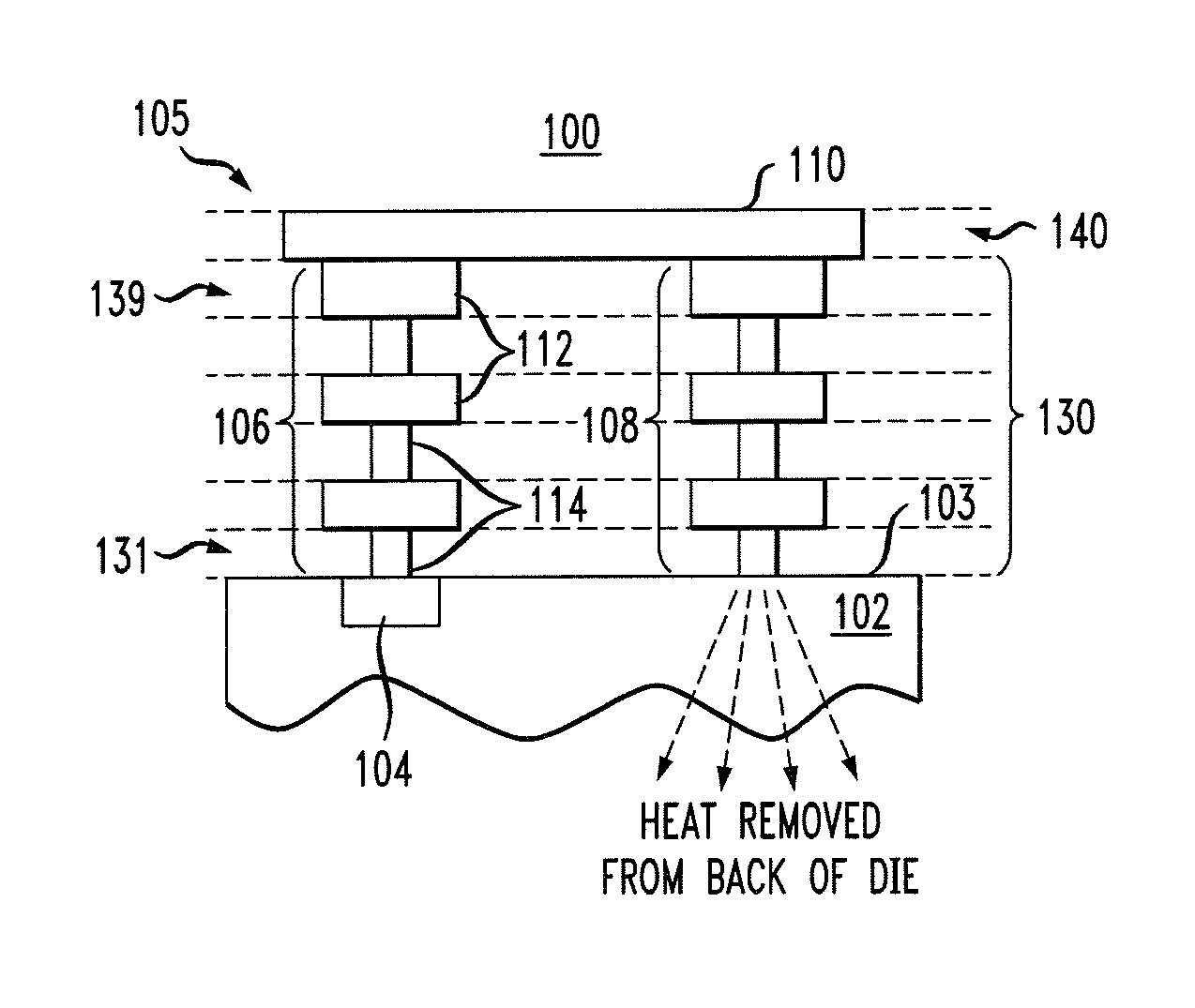
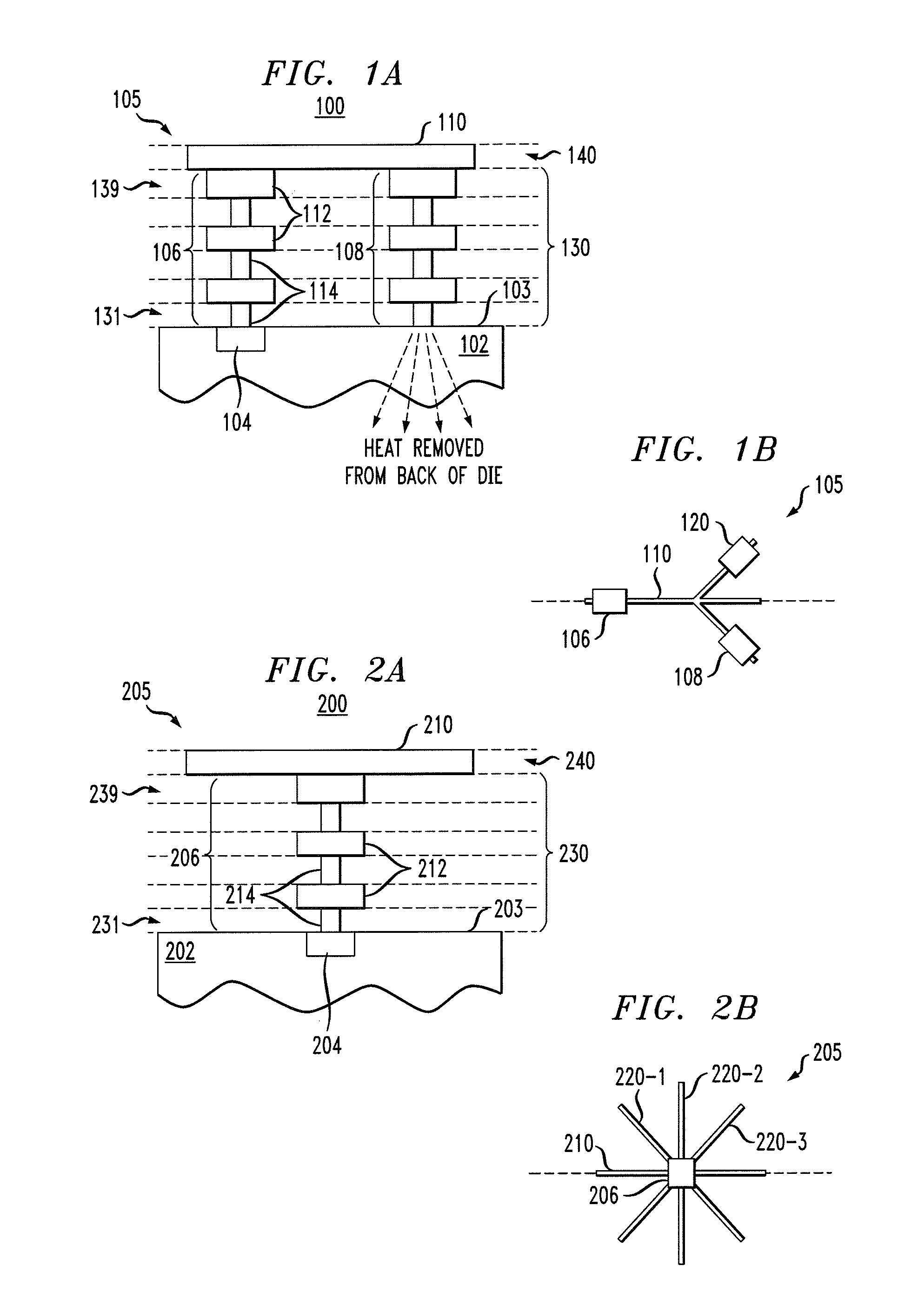
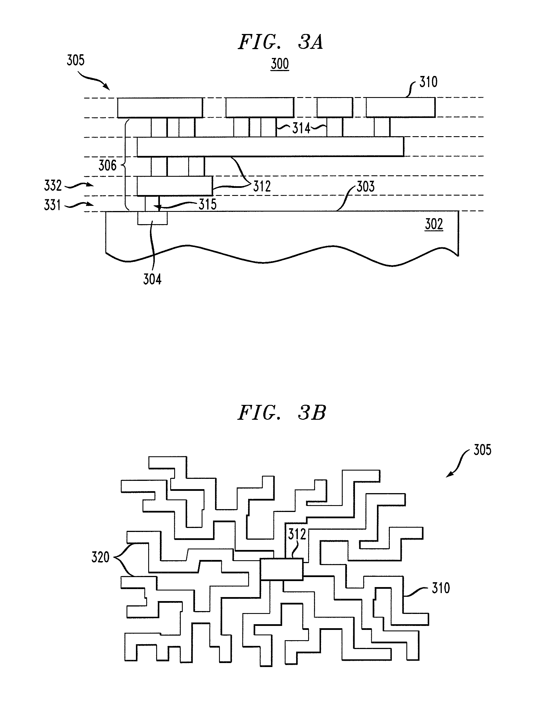
[0020]The present invention will be illustrated herein in the context of exemplary integrated circuit arrangements comprising heat conducting structures. It is to be appreciated that the particular circuit arrangements and associated heat conducting structures shown in the illustrative embodiments are presented by way of example only. Accordingly, the invention should not be construed as requiring any particular aspects of these exemplary elements.

[0021]The term “integrated circuit die” as used herein may comprise any type of device wherein electrical circuits are fabricated in or on a semiconductor substrate. A given integrated circuit die may be of any type including analog, digital or mixed signal. Furthermore, a given die may comprise electrical circuits of any type, configuration and dimension.

[0022]The term “substrate” comprises any type of crystalline semiconductor material and is not limited to that formed of silicon. Optionally, other materials may be used such as gallium a...


PUM


Abstract

An integrated circuit die includes a substrate having an upper surface, at least one active device formed in a first area of the upper surface of the substrate, and a plurality of layers formed on the upper surface of the substrate above the at least one active device. A first stacked heat conducting structure is provided, spanning from a point proximate the first area of the upper surface of the substrate through the plurality of layers. A lateral heat conducting structure is formed above the uppermost layer of the plurality of layers and in thermal contact with the first stacked heat conducting structure. The invention advantageously facilitates the dissipation of heat from the integrated circuit die, particularly from high-power sources or other localized hot spots.

Description

FIELD OF THE INVENTION[0001]This invention relates generally to integrated circuits, and more specifically to techniques for controlling heat dissipation in integrated circuits.BACKGROUND OF THE INVENTION[0002]With advances in semiconductor design and fabrication, the circuit density that can be implemented on a given integrated circuit die has steadily increased, leading to higher power consumption and heat generation. Simultaneously, the scaling to finer geometries has exacerbated issues such as sub-threshold leakage current, making the circuits more susceptible to performance degradation due to temperature variations across the die. Thus, it is becoming increasingly important to efficiently remove heat from an integrated circuit die in order to avoid temperature induced failures.[0003]A typical approach to removing heat from an integrated circuit die is to attach a heat sink to the exterior of the semiconductor packaging. A heat sink is commonly understood to increase the dissipa...

Claims


Application Information

Patent Timeline
Patent Type & Authority Patents(United States)
IPC IPC(8): H01L23/48H01L23/34H01L21/20H01L23/52H01L23/12H01L23/053H01L29/40H01L21/4763H01L21/00H01L21/44
CPCH01L23/367H01L2924/0002H01L2924/00
Inventor RYAN, VIVIAN
Owner BELL SEMICON LLC
Why Eureka
Try Eureka