Method for Growing III-V Epitaxial Layers

Active Publication Date: 2014-06-19
EPIGAN NV
View PDF5 Cites 11 Cited by
  • Summary
  • Abstract
  • Description
  • Claims
  • Application Information

AI Technical Summary

Benefits of technology

[0044]Another object of the invention is to facilitate stress engineering when depositing III-nitride layers on a foreign substrate. Because the breakdown voltage of the semiconductor structure is not limited by the conductive layer once suitable iso

Problems solved by technology

This breakdown is due to the undesired generation of a conductive path at the interface between Si substrate and III-nitrid

Method used


Image

  • Method for Growing III-V Epitaxial Layers
  • Method for Growing III-V Epitaxial Layers
  • Method for Growing III-V Epitaxial Layers

Examples


Embodiment Construction

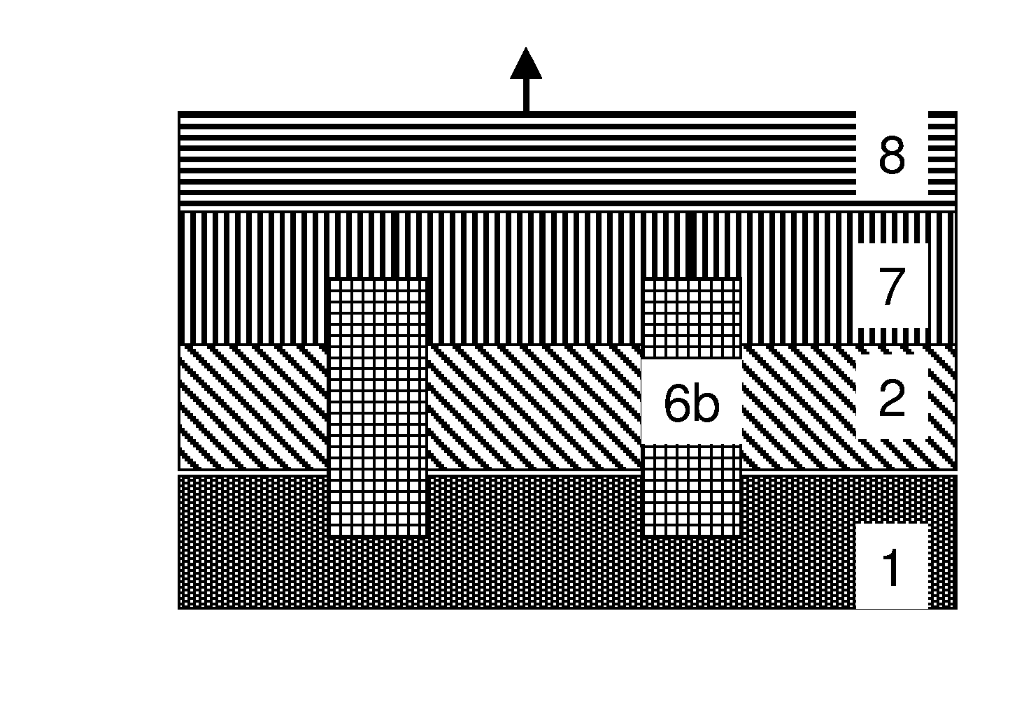
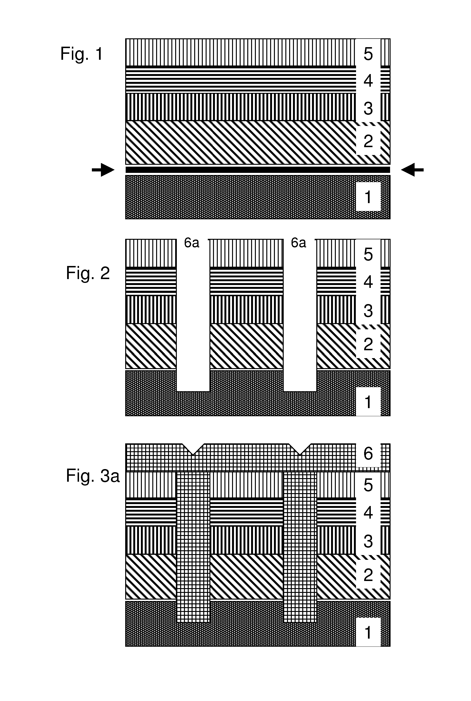
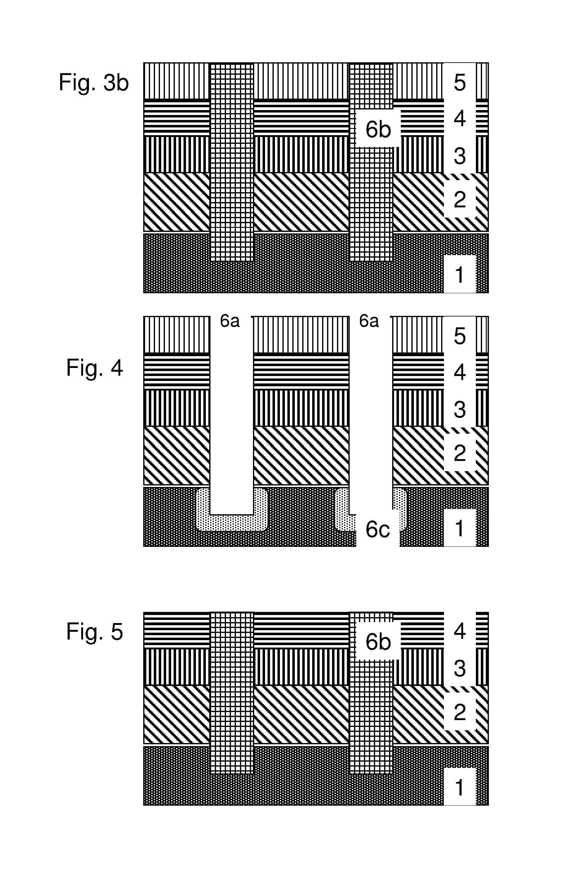
[0047]The present invention will be described with respect to particular embodiments and with reference to certain drawings but the invention is not limited thereto but only by the claims. The drawings described are only schematic and are non-limiting. In the drawings, the size of some of the elements may be exaggerated and not drawn on scale for illustrative purposes. The dimensions and the relative dimensions do not correspond to actual reductions to practice of the invention.

[0048]In a first aspect the present invention relates to a method of manufacturing a semiconductor structure comprising[0049]providing a substrate, such as a Si, SiGe, Ge, substrate, and combinations thereof, preferably a Si substrate, such as a Si substrate,[0050]providing an epitaxial semiconducting buffer layer on top of the substrate, such as a III-V buffer layer, thus forming an interface, and[0051]forming one or more local electrical isolations in the substrate at the interface, such as a shallow trenc...


PUM


Abstract

Disclosed are methods of growing III-V epitaxial layers on a substrate, semiconductor structures thus obtained, and devices comprising such semiconductor structures. An example semiconductor substrate includes a substrate and a buffer layer on top of the substrate, where a conductive path is present between the substrate and buffer layer. A conductive path may be present in the conductive interface, and the conductive path may be interrupted by one or more local electrical isolations. The local electrical isolation(s) may be positioned with the device such that at least one of the local electrical isolation(s) is located between a high voltage terminal and a low voltage terminal of the device.

Description

CROSS-REFERENCE TO RELATED APPLICATIONS[0001]The present application is a national stage entry of PCT / EP2012 / 063317, filed Jul. 6, 2012, which claims priority to Great Britain Patent Application Serial No. 1112327.0 filed Jul. 18, 2011. The full disclosures of Great Britain Patent Application Serial No. 1112327.0 and PCT / EP2012 / 063317 are hereby incorporated herein by reference.FIELD OF THE INVENTION[0002]The present invention relates to a method of growing III-V epitaxial layers on a substrate, a semiconductor structure comprising a substrate, a buffer layer on top of the substrate, wherein a conductive path is present between the substrate and buffer layer, and a device comprising such a structure.TECHNICAL BACKGROUND[0003]When depositing for instance III-N epitaxial layers on Si substrates, growth is started with the deposition of an AlN layer to suppress the so-called “Ga melt-back” of the Si substrates. At the interface between the Si and the AlN, a conductive layer is formed, ...

Claims


Application Information

Patent Timeline
IPC IPC(8): H01L21/02H01L29/778H01L29/66
CPCH01L21/02538H01L29/778H01L29/66431H01L29/0649H01L21/0254H01L21/02636H01L21/30612H01L21/31051H01L21/76202H01L21/76213H01L21/76224H01L29/2003H01L29/205H01L29/7787
Inventor DERLUYN, JOFFDEGROOTE, STEFANGERMAIN, MARIANNE
Owner EPIGAN NV
Why Eureka
Try Eureka