Conversion of high-energy photons into electricity

a high-energy photon and conversion technology, applied in the field of photonic energy conversion, can solve the problems of difficulty in providing such devices, and no known devices for converting into electricity energy from photons operating in the high-energy photon regim

Active Publication Date: 2013-05-23
TAE TECH INC +1
View PDF1 Cites 22 Cited by
  • Summary
  • Abstract
  • Description
  • Claims
  • Application Information

AI Technical Summary

Benefits of technology

[0006]The systems and methods provided herein utilize a series of materials with differing atomic charges to take advantage of the emission of a large multiplicity of electrons by a single high-energy photon via a cascade of Auger electron emissions. In one embodiment, a high-energy photon converter preferably includes a linearly layered nanometric-scaled wafer made up of a first plurality of layers of a material for absorbing high energy photons and emitting electrons combined with a second plurality of layers of other materials for absorbing or collecting electrons. The material of the second plurality of layers having an atomic charge number differing from the atomic charge number of the material of the first plurality of layers. The first and second plurality of layers are preferably stacked laterally side-by-side (i.e., face-to-face), interposing one another, and oriented at a grazing (shallow) angle to the direction of the propagation of the high energy photons. In another embodiment, the nanometric-scaled layers are configured in a tubular or shell-like configuration. In yet another embodiment, the layers include a third plurality of layers of insulator material.
[0007]The systems and methods described herein may be utilized in a wide range of applications—from energy detection and absorption, to energy conversion of high-energy photons in particle accelerators and from other extremely hot matter (such as high temperature plasmas) and / or detonation sources that emit copious high-energy photons (such as explosives), energy capture of emissions of radioactive nuclear wastes (such as spent fission fuel rods), and space applications (such as power sources, shielding, and the like), as well as other applications readily recognizable to one skilled in the art.

Problems solved by technology

There are, however, no known devices for conversion into electricity of energy from photons operating in the high-energy photon regime such as, e.g., XUV, X and gamma rays.
Difficulties in providing such devices arise from the great penetrability of high-energy photons through matter, which is a consequence of much less interaction of such photons with matter when compared with visible light, and from the fact that for most materials the mean-free-path of electrons is typically many orders of magnitude shorter than the mean-free-path of high-energy photons.

Method used


Image

  • Conversion of high-energy photons into electricity
  • Conversion of high-energy photons into electricity
  • Conversion of high-energy photons into electricity

Examples


Embodiment Construction

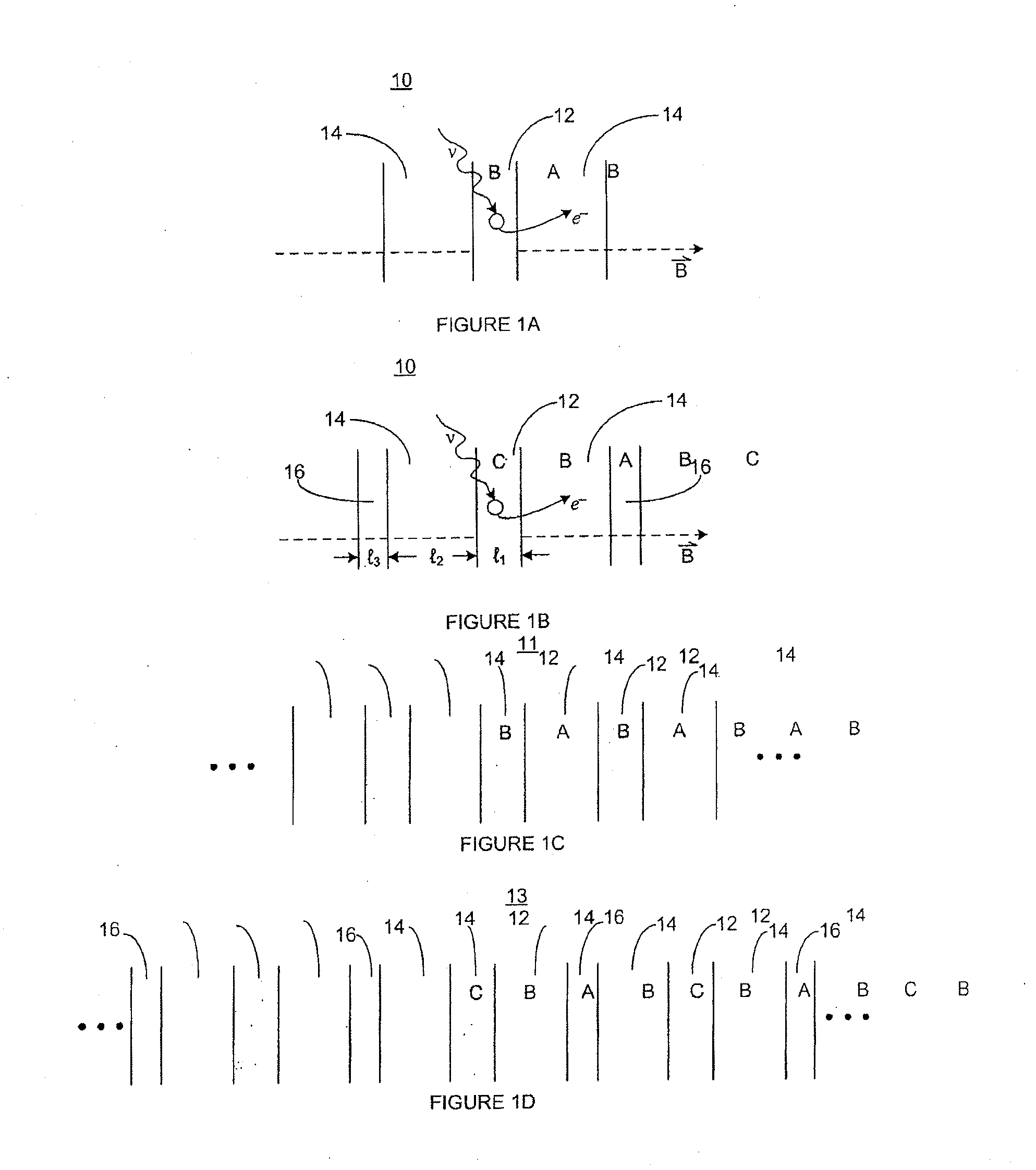
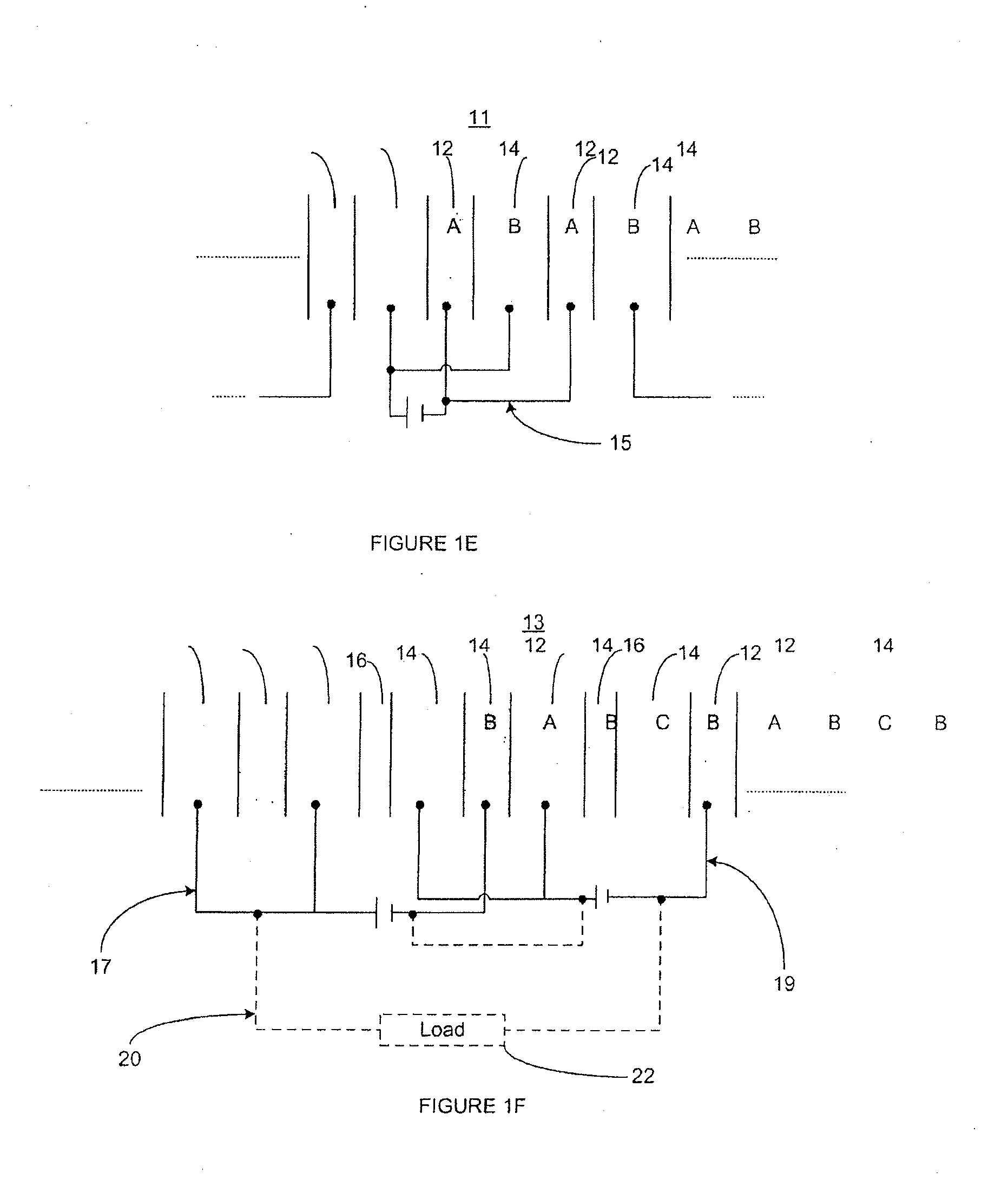
[0027]Each of the additional features and teachings disclosed below can be utilized separately or in conjunction with other features and teachings to produce systems and methods to facilitate the conversion of energy from high-energy photons into electricity. Representative examples of the present invention, which examples utilize many of these additional features and teachings both separately and in combination, will now be described in further detail with reference to the attached drawings. This detailed description is merely intended to teach a person of skill in the art further details for practicing preferred aspects of the present teachings and is not intended to limit the scope of the invention. Therefore, combinations of features and steps disclosed in the following detail description may not be necessary to practice the invention in the broadest sense, and are instead taught merely to particularly describe representative examples of the present teachings.

[0028]Moreover, the...


PUM


Abstract

Systems and methods for the conversion of energy of high-energy photons into electricity which utilize a series of materials with differing atomic charges to take advantage of the emission of a large multiplicity of electrons by a single high-energy photon via a cascade of Auger electron emissions. In one embodiment, a high-energy photon converter preferably includes a linearly layered nanometric-scaled wafer made up of layers of a first material sandwiched between layers of a second material having an atomic charge number differing from the atomic charge number of the first material. In other embodiments, the nanometric-scaled layers are configured in a tubular or shell-like configuration and / or include layers of a third insulator material.

Description

FIELD[0001]The embodiments described herein relate generally to photonic energy conversion and, more particularly, to systems and methods that facilitate the conversion of energy from high-energy photons into electricity.BACKGROUND INFORMATION[0002]There exist many well-known devices that convert the energy of photons in the optical range into electricity, such as, e.g., photovoltaic cells (‘solar cells’). These devices are generally made up of at least two materials (i.e. silicon-based semiconductors) with different physical properties, such as different electron affinities (see, P. Würfel, The Physics of Solar Cells, 1st Edition, Wiley-VCH (2004)). When one of the materials is illuminated by sunshine, solar photons excite photoelectrons from a valence band into a conduction band, which provides electric mobility. The energy gap between valence and conduction bands is typically on the order of an electron-volt, which is similar to the energy of the incident solar photons. The arran...

Claims


Application Information

Patent Timeline
Patent Type & Authority Applications(United States)
IPC IPC(8): H01L31/0725
CPCG01T1/28G21H1/06H01L31/0725H01L31/115H01L31/0352H01L31/02H01L31/0232H01L31/0256G21H1/04Y02E10/50H01L31/085Y02E10/542
Inventor BINDERBAUER, MICHLTAJIMA, TOSHIKI
Owner TAE TECH INC
Why Eureka
Try Eureka