Liquid crystal display device and manufacturing method thereof

a liquid crystal display and manufacturing method technology, applied in the manufacture of electrode systems, electric discharge tubes/lamps, instruments, etc., can solve the problems of reducing the stability of alignment treatment compared with rubbing treatment, display failure, and display failure typically represented by residual images, so as to improve residual image characteristics, reduce alignment film resistance, and excellent image quality

Active Publication Date: 2013-05-23
JAPAN DISPLAY INC
View PDF3 Cites 9 Cited by
  • Summary
  • Abstract
  • Description
  • Claims
  • Application Information

AI Technical Summary

Benefits of technology

[0022]According to the present invention, since charges are rendered to be moved easily or the resistance of the alignment film is lowered in a region not irradiated with the bac

Problems solved by technology

However, in view of the provision of the alignment controllability to the alignment film, it has been known that the optical alignment treatment generally has lower alignment stability compared with the rubbing treatment.
If the align

Method used


Image

  • Liquid crystal display device and manufacturing method thereof
  • Liquid crystal display device and manufacturing method thereof
  • Liquid crystal display device and manufacturing method thereof

Examples


first embodiment

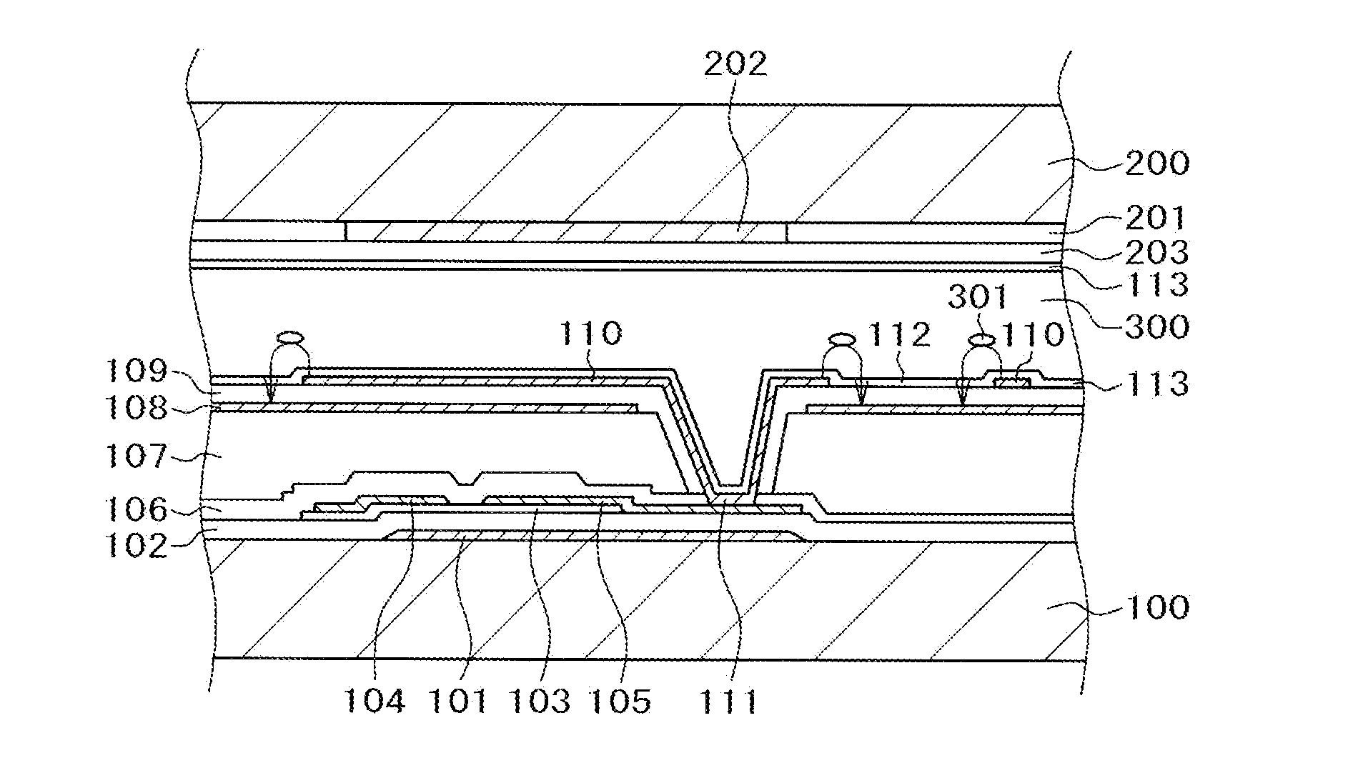
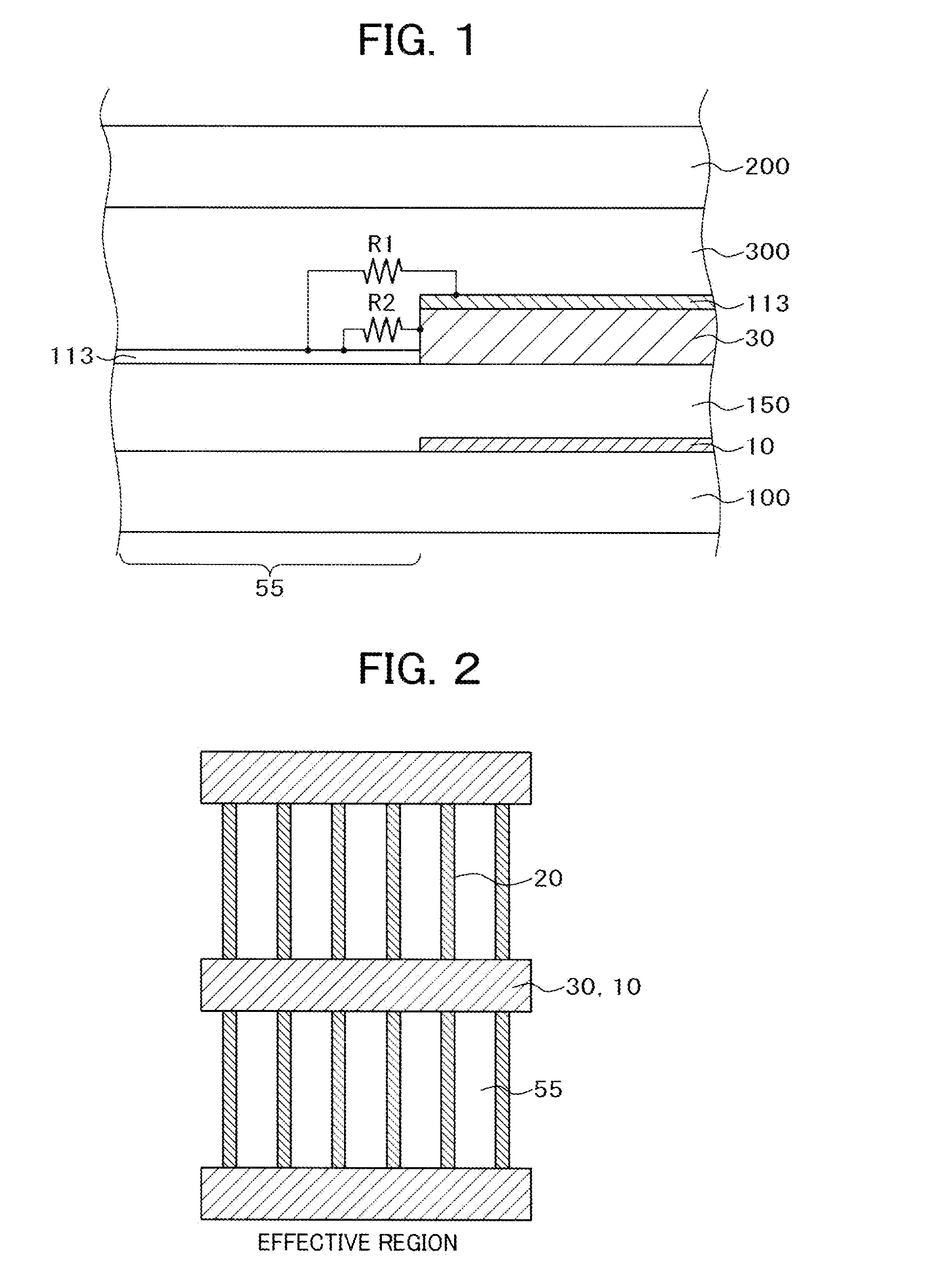
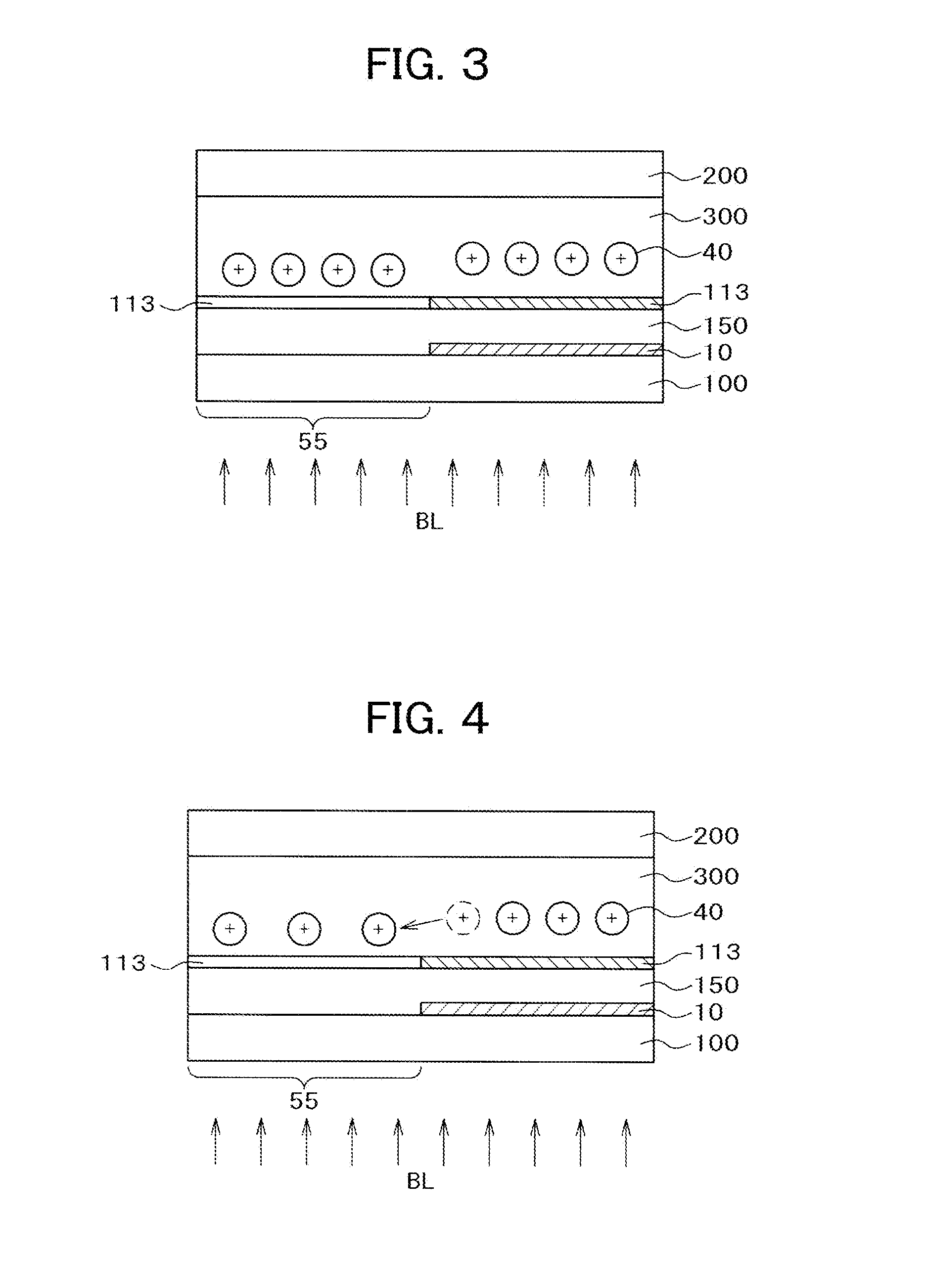
[0058]FIG. 1 is a cross sectional view showing a configuration of a first embodiment of the invention and FIG. 2 is a plan view of the first embodiment. Prior to explanation of FIG. 1 and FIG. 2, a mechanism that a residual image is present for a long time is to be described with reference to FIG. 3 to FIG. 6. The residual image includes a so-called DC residual image of sticking and gradual elimination of a pattern when an identical image is displayed for a predetermined pattern, and a so-called AC residual image caused by lowering of the alignment performance of the alignment film. The invention provides a countermeasure against the so-called DC residual image.

[0059]FIG. 3 shows a state in which electric charges are accumulated on the surface of an alignment film 113 just after display of a predetermined pattern. In FIG. 3, a gate line 10 is formed over a TFT substrate 100, an intermediate layer 150 comprising various insulation layers such as a gate insulation film, an inorganic p...

second embodiment

[0077]FIG. 11 is a cross sectional view showing a configuration of a second embodiment of the invention in a display region and FIG. 12 is a plan view thereof. In the existent embodiment shown in FIG. 6, since no photoconductive effect is obtainable in the shielded portion of the alignment film 113, a problem exists in that the charges accumulated in the shielded portion cannot rapidly transfer to the opening portion due to high resistance. This embodiment has a feature of originally lowering the resistance in the shielded portion of the alignment film 113, even though the photoconductive effect cannot be obtained.

[0078]In the configuration of the second embodiment shown in FIG. 11, after an alignment film 113 is formed, an opening portion 55 is shielded by using a photomask 80 and UV-light is applied only to the shielded portion. A TFT substrate 100 formed with the alignment film 113 is placed over a hot plate 70 and the substrate is heated to 200° C. to 210° C. at the same time wi...


PUM


Abstract

A high quality liquid crystal display device has an alignment film with a photoconductive characteristic. Since a region having gate lines situated therebelow does not undergo irradiation of a backlight, no photoconductive effect can be obtained. A photoresist is disposed below the alignment film situated over the gate lines in order to transfer the charges in the region to an opening portion of the alignment film in an early stage. Since the photoresist has a thickness of about 1.5 μm, which is 20 times or more the 70 nm thickness of the alignment film, the resistance in the lateral direction is low in a portion where the photoresist is present. Accordingly, since the charges on the alignment film present over the gate line transfer to the opening portion of the alignment film and are eliminated in an early stage, the residual image is eliminated in the early stage.

Description

CLAIM OF PRIORITY[0001]The present application claims priority from Japanese Patent Application JP 2011-2535287 filed on Nov. 21, 2011, the content of which is hereby incorporated by reference into this application.BACKGROUND OF THE INVENTION[0002]1. Field of the Invention[0003]The present invention relates to a liquid crystal display device, and particularly relates to a liquid crystal display device having a liquid crystal display panel of which alignment film is provided with alignment controllability by irradiation of light.[0004]2. Description of the Related Art[0005]Liquid crystal display devices include a TFT substrate having pixel electrodes, thin film transistors (TFT), etc. formed in a matrix; a counter substrate disposed in facing relation to the TFT substrate and having color filters, etc. formed at positions corresponding to the pixel electrodes of the TFT substrate; and liquid crystals put between the TFT substrate and the counter substrate. Images are formed by contro...

Claims


Application Information

Patent Timeline
IPC IPC(8): G02F1/1335G02F1/13
CPCG02F1/1303G02F1/133602G02F2001/133397G02F2001/133388G02F1/133788G02F1/133388G02F1/133397G02F1/1337
Inventor MATSUI, CHIKAEKUNIMATSU, NOBORUSONODA, HIDEHIRO
Owner JAPAN DISPLAY INC
Why Eureka
Try Eureka