Electrode paste composition, electrode for electronic device using the same, and method of manufacturing the same

a technology of electronic devices and electrodes, applied in the direction of instruments, applications, conductors, etc., can solve the problems of difficult application of indium tin oxide to flexible electronic devices, increased manufacturing costs, and difficulty in achieving uniform resistivity and electrical conductivity. , to achieve the effect of excellent uniform resistivity and electrical conductivity

Inactive Publication Date: 2013-05-23
SAMSUNG ELECTRO MECHANICS CO LTD
View PDF4 Cites 5 Cited by
  • Summary
  • Abstract
  • Description
  • Claims
  • Application Information

AI Technical Summary

Benefits of technology

[0014]An aspect of the present invention provides an electrode paste composition having excellent uniform resistivity and electrical conductivity, an electrode for an electronic device using the same, and a method of manufacturing the same.

Problems solved by technology

However, since manufacturing costs may be increased due to price increases and the limited supply of its main material, indium (In), as well as the fact that indium tin oxide is inflexible, indium tin oxide is difficult to apply to a flexible electronic device.
As for the method of refining graphite to produce the graphene thin film, a high-quality graphene thin film may be obtained but a process procedure may be somewhat complex.
However, the method using graphene oxide to manufacture the electrode causes electrical properties to be more degraded than is the case with the use pure graphene, and the electrode may be manufactured in small pieces instead of a single thin film, thereby deteriorating properties thereof suitable for the formation of a transparent electrode.
Meanwhile, pure graphene is difficult to disperse in a dispersive solvent, thereby deteriorating uniform resistivity of an electrode.

Method used


Image

  • Electrode paste composition, electrode for electronic device using the same, and method of manufacturing the same
  • Electrode paste composition, electrode for electronic device using the same, and method of manufacturing the same
  • Electrode paste composition, electrode for electronic device using the same, and method of manufacturing the same

Examples


Embodiment Construction

[0033]Exemplary embodiments of the present invention will now be described in detail with reference to the accompanying drawings. The invention may, however, be embodied in many different forms and should not be construed as being limited to the embodiments set forth herein. Rather, these embodiments are provided so that this disclosure will be thorough and complete, and will fully convey the scope of the invention to those skilled in the art. In the drawings, the shapes and dimensions of some components may be exaggerated for clarity, and the same reference numerals will be used throughout to designate the same or like components.

[0034]Embodiments of the present invention will now be described in detail with reference to the accompanying drawings.

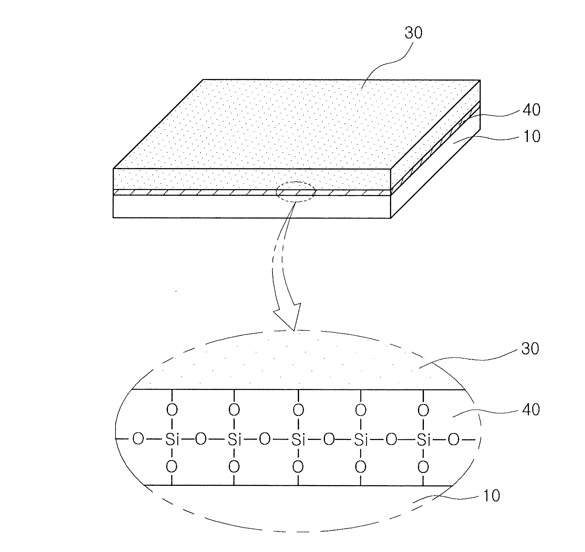
[0035]FIG. 1 shows a schematic perspective view and a schematic partial enlarged view of an electrode for an electronic device according to an embodiment of the present invention.

[0036]Referring to FIG. 1, an electrode for an electronic de...


PUM

PropertyMeasurementUnit
thicknessaaaaaaaaaa
transparentaaaaaaaaaa
polaraaaaaaaaaa

Abstract

There is provided an electrode paste composition, an electrode for an electronic device using the same, and a method of manufacturing the same. The electrode for an electronic device includes: a substrate; a thin film layer formed on the substrate, the thin film layer including reduced graphene oxide (rGO); and an oxide layer formed between the substrate and the thin film layer. The electrode for an electronic device may have excellent uniform resistivity and electrical conductivity since the electrode is formed by coating the substrate with a solution containing graphene oxide having superior dispersibility and reducing the graphene oxide.

Description

CROSS-REFERENCE TO RELATED APPLICATIONS[0001]This application claims the priority of Korean Patent Application Nos. 10-2011-0121627 filed on Nov. 21, 2011 and 10-2011-0138525 filed on Dec. 20, 2011, in the Korean Intellectual Property Office, the disclosures of which are incorporated herein by reference.BACKGROUND OF THE INVENTION[0002]1. Field of the Invention[0003]The present invention relates to an electrode paste composition having excellent uniform resistivity and electrical conductivity, an electrode for an electronic device using the same, and a method of manufacturing the same.[0004]2. Description of the Related Art[0005]Graphene is a material in which carbon atoms are arranged two-dimensionally. Unlike graphite, graphene is formed to be extremely thin with a structure having a single layer of carbon atoms, or two or three layers thereof.[0006]Since graphene is flexible and transparent, as well as having very high electrical conductivity, studies into using graphene as a tra...

Claims


Application Information

Patent Timeline
Patent Type & Authority Applications(United States)
IPC IPC(8): H01B1/00B32B5/16B32B15/02H01B1/20B32B9/04B05D5/12B82Y30/00B82Y40/00B82Y99/00
CPCB32B5/16B32B9/04B32B15/02Y10T428/265H01B1/22C09D11/52C23C18/1212B82Y30/00Y10T428/31678
Inventor KIM, WOON CHUNHUR, KANG HEON
Owner SAMSUNG ELECTRO MECHANICS CO LTD
Why Eureka
Try Eureka