Eureka AIR delivers breakthrough ideas for toughest innovation challenges, trusted by R&D personnel around the world.

Data read/write system

Active Publication Date: 2013-05-23
MONTAGE TECHNOLOGY CO LTD
View PDF4 Cites 23 Cited by
  • Summary
  • Abstract
  • Description
  • Claims
  • Application Information

AI Technical Summary

Benefits of technology

The data read / write system described in this patent helps to reduce power consumption when reading and writing data to memory chips, specifically tries to reduce power consumption in DDR4 X4 memory chips. This is achieved by controlling the inversion of data on a specific line called the data bus inversion control line (DBI). This system can make the interface between the memory chip and the rest of the computer more efficient, which can improve performance and reduce energy consumption.

Problems solved by technology

Since the working frequency of the DDR4 memory chip is high, an error rate of a data read / write operation is greatly increased.
Therefore, how to read data from a DDR4 X4 memory chip or write data into the DDR4 X4 memory chip becomes a problem to be solved by those skilled in the art.

Method used


Image

  • Data read/write system
  • Data read/write system
  • Data read/write system

Examples


Embodiment Construction

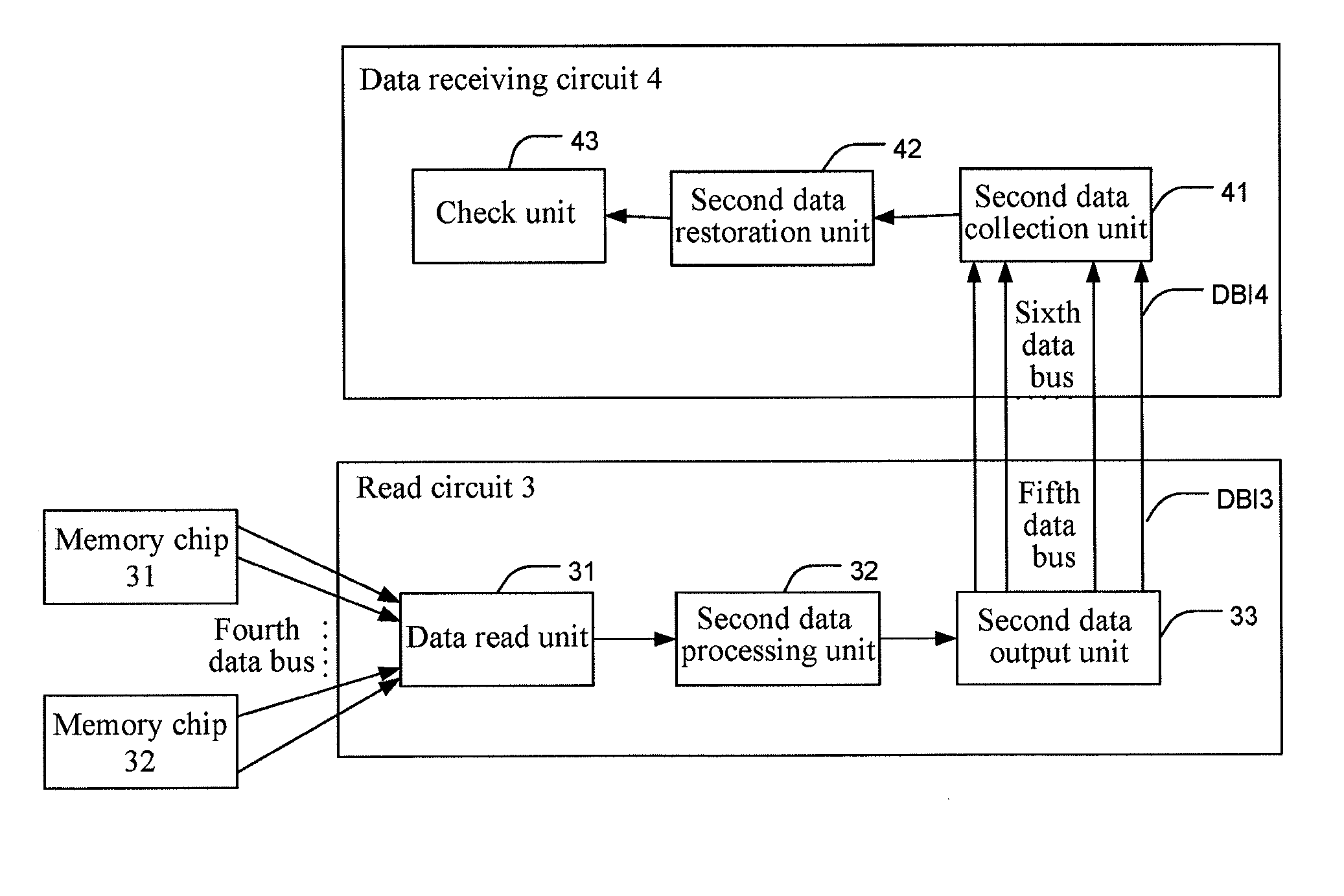
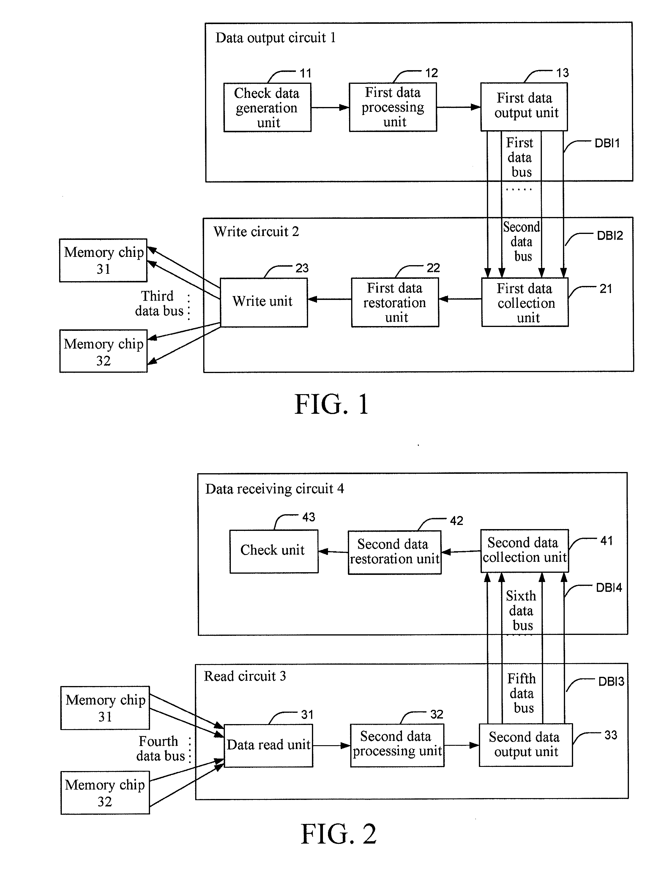
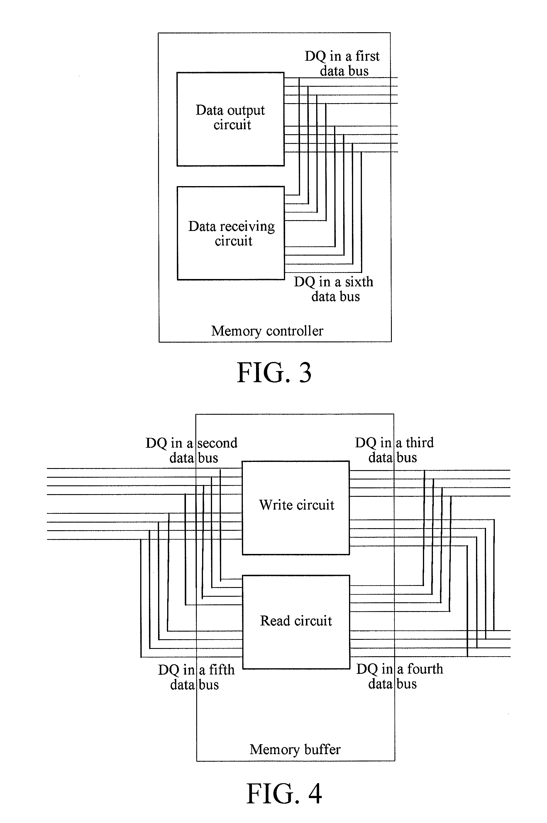
[0035]FIG. 1 is a schematic diagram of a data read / write system for writing data into a memory chip according to a preferred embodiment of the present invention. The data read / write system includes a data output circuit 1 and a write circuit 2. The data output circuit 1 includes a check data generation unit 11, a first data processing unit 12, and a first data output unit 13. The write circuit 2 includes a first data collection unit 21, a first data restoration unit 22 and a write unit 23.

[0036]The check data generation unit 11 is configured to generate a first set of check data according to n1*b pieces of data in n*b pieces of data to be output and generate a second set of check data according to the remaining n2*b pieces of data in the n*b pieces of data to be output.

[0037]A circuit structure of the check data generation unit 11 is determined according to a pre-determined method adopted to generate the first set of check data and the second set of check data. For example, if it is...


PUM


Abstract

The present invention provides a data read / write system. The data read / write system includes a memory controller and a memory module. The memory controller includes a first control circuit, a data output circuit, and a data receiving circuit. The memory module includes a memory buffer and at least two memory chips. The memory buffer includes a second control circuit, a write circuit, and a read circuit. The advantage of the present invention is that, when data is read or written into the memory chip, especially a DDR4 X4 memory chip, low power consumption of interface data transmission can be achieved through a data bus inversion control line DBI.

Description

BACKGROUND OF THE PRESENT INVENTION[0001]1. Field of Invention[0002]The present invention relates to the field of computers, and specifically to a data read / write system.[0003]2. Description of Related Arts[0004]The DDR4 SDRAM is the next generation synchronous dynamic random access memory technology. In contrast to the prior SDRAM technology, the DDR4 is revolutionarily changed. In the new generation DDR4 SDRAM, the Through Silicon Via (TSV) technology and a multi-layer manufacturing process (4 stacks or 8 stacks) may be used, thereby greatly increasing the capacity of a memory chip. The DDR4 works in a frequency range from 1600 MHz to 3200 MHz, which may also be expanded to a frequency range from 2133 MHz to 4266 MHz, and a working voltage of the DDR4 is even reduced to a voltage range from 1.05 V to 1.25 V. Moreover, in the DDR4, the number of banks is increased, and an input / output interface circuit is improved. In contrast to the DDR3 SDRAM, the DDR4 has many advantages such as...

Claims


Application Information

Patent Timeline
IPC IPC(8): G06F12/00G06F12/02
CPCG06F12/00G06F12/0246G06F11/1004
Inventor LI, HAIYANGMA, QINGJIANG
Owner MONTAGE TECHNOLOGY CO LTD
Why Eureka
Eureka Blog
Learn More