Equipment for Making IC Shielding Coating Layer and Metal Shielding Layer of IC

a technology of ic shielding and coating layer, which is applied in the direction of electrolysis components, vacuum evaporation coatings, coatings, etc., can solve the problems of high manufacturing cost, high complexity and density of ic, and possible electromagnetic interference (emi) with other electronic components, so as to achieve effective cost reduction and reduce manufacturing time

Inactive Publication Date: 2013-05-30
CHENMING MOLD IND CORP
View PDF17 Cites 8 Cited by
  • Summary
  • Abstract
  • Description
  • Claims
  • Application Information

AI Technical Summary

Benefits of technology

[0023](1) The equipment for making IC shielding coating layer uses a PVD process to sputter one or more layers of metal materials onto a surface of an IC to form a metal shielding layer, so that the IC has an electromagnetic shielding effect. It is no longer to use a metal cover plate for shielding anymore, so that the assembling of the metal cover plate is not required. The layer coating method is used for forming the metal shielding, so that it is no need to consider the corresponding dimensions of the IC and the metal cover plate, and the cost can be lowered effectively.
[0024](2) When the equipment for making IC shielding coating layer is used for performing the layer coating of an IC, all manufacturing processes are finished inside the chamber without the need of transportation or moving, and the work support in the equipment is designed with a multi-axis revolution and rotation structure, and the work support can be used for putting a plurality of ICs, and many medium frequency magnetron targets and multi-arc ion targets are disposed at different points on the external side of the work support, so as to expedite the layer coating of the IC and lower the manufacturing time.
[0025](3) The equipment for making IC shielding coating layer further uses the medium frequency magnetron targets and multi-arc ion targets to sputter an oxide, a nitride, a carbide, or a compound with a combination of the above over the final layer on the metal shielding layer to form an insulating layer after the metal shielding layer completes sputtering the metal material over the IC. The insulating layer can prevent the solder from touching the metal shielding layer during the soldering process, which may result in a short circuit caused by the contact between the metal shielding layer and the circuit.

Problems solved by technology

Therefore, the complexity and density of the integrated circuit (IC) become higher, the conductive transmission wire and the power supply or other components having a higher working frequency installed on the printed circuit board will produce electromagnetic waves, so that an electromagnetic interference (EMI) with other electronic components may occur.
Therefore, it is an important issue to find a way to overcome the influence of electromagnetic interference on the circuit.
Since the metal casing 11 is assembled onto the printed circuit board 1 by independent manufacturing processes and additional labor, the manufacturing cost is very high.
When it is necessary to maintain, repair or replace the IC chip 12, the metal casing 11 must be removed first, and thus it is very inconvenient and easy to damage the printed circuit board 1.
In addition, the heat dissipation is also a major issue.
With reference to FIG. 2 for another conventional IC shielding layer, a shielding layer 21 is formed on a printed circuit board 2 having a plurality of IC chips 22, and this manufacturing method requires a process of forming the shielding layer 21 on the printed circuit board 2, and thus ruining the original manufacturing process, and causing tremendous inconvenience.
In addition, this manufacturing method can form the shielding layer on a plurality of IC chips, and slice into single IC chips for use, and the shielding layer cannot be formed directly on the single IC chip, and the flexibility is limited.

Method used


Image

  • Equipment for Making IC Shielding Coating Layer and Metal Shielding Layer of IC
  • Equipment for Making IC Shielding Coating Layer and Metal Shielding Layer of IC
  • Equipment for Making IC Shielding Coating Layer and Metal Shielding Layer of IC

Examples


Embodiment Construction

[0031]The technical characteristics of the present invention will become clear with the detailed description of the preferred embodiments accompanied with the illustration of related drawings as follows. It is noteworthy to point out that the drawings are provided for the purpose of illustrating the present invention and supporting the description of the specification only, but not intended for limiting the scope of the invention, and the drawings are not necessarily drawn with actual proportion and precision.

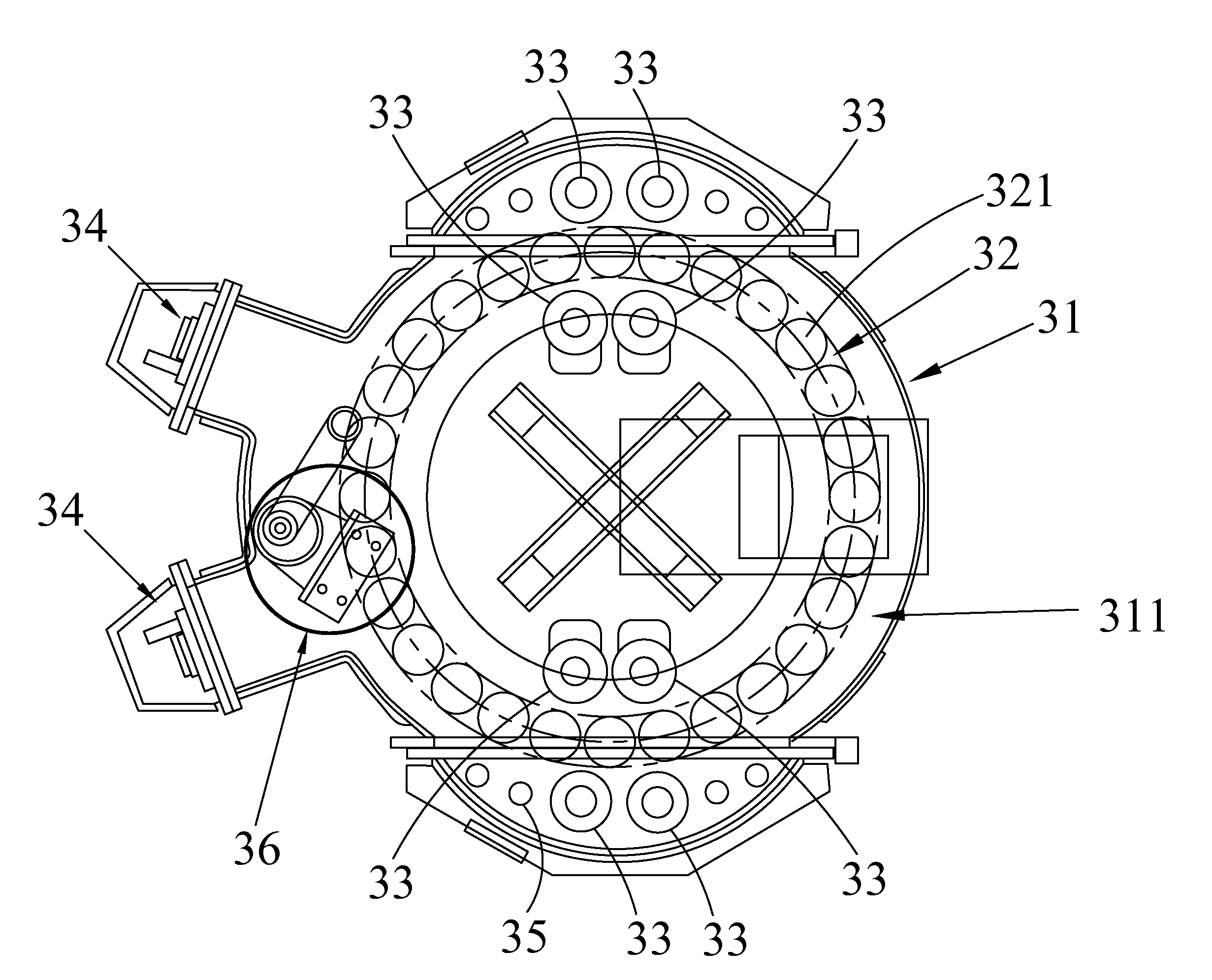
[0032]With reference to FIG. 3 for a schematic view of equipment for making IC shielding coating layer in accordance with a preferred embodiment of the present invention. The equipment for making an IC shielding coating layer comprises a base 31, a work support 32, a plurality of medium frequency magnetron targets 33, a plurality of multi-arc ion targets 34, a plurality of heating pipes 35, bias / driving equipment 36 and vacuum equipment (not shown in the figure), wherein the pl...


PUM

PropertyMeasurementUnit
temperatureaaaaaaaaaa
pulse voltageaaaaaaaaaa

Abstract

Equipment for making IC shielding coating layer and a metal shielding layer of IC. The equipment comprises a base, a work support, a plurality of medium frequency magnetron targets and a plurality of multi-arc ion targets. The base comprises a chamber. The work support is disposed in the chamber and movably connected with a plurality of rotation axes. Each rotation axes comprises at least one fixture. The fixture is used to put at least one IC. Each medium frequency magnetron target and each multi-arc ion target are disposed in the chamber. The medium frequency magnetron targets and the multi-arc ion targets are used to sputter a metal material over the IC to form at least one metal shielding layer on a surface of the IC.

Description

CROSS-REFERENCE TO RELATED APPLICATION[0001]This application claims the benefit of Taiwan Patent Application No. 100143653, filed on Nov. 29, 2011, in the Taiwan Intellectual Property Office, the disclosure of which is incorporated herein in its entirety by reference.BACKGROUND OF THE INVENTION[0002]1. Field of the Invention[0003]The present invention relates to equipment for making IC shielding coating layer and a metal shielding layer of IC, in particular to the equipment for making IC shielding coating layer and the metal shielding layer of IC by using a physical vapor deposition (PVD) process to produce an IC with a surface with an electromagnetic shielding effect.[0004]2. Description of the Related Art[0005]As science and technology advance, the electronic product has an increasingly smaller size and an increasing powerful function. Therefore, the complexity and density of the integrated circuit (IC) become higher, the conductive transmission wire and the power supply or other ...

Claims


Application Information

Patent Timeline
Patent Type & Authority Applications(United States)
IPC IPC(8): C23C14/35C23C14/58
CPCH01J37/32055H01J37/3405H01J37/3429H05K9/0032C23C14/505C23C14/025C23C14/06C23C14/325C23C14/352C23C14/021
Inventor LIU, CHAO-LUNCHIOU, YAU-HUNGFAN, SHU-HUI
Owner CHENMING MOLD IND CORP
Why Eureka
Try Eureka