Tungsten film forming method

a technology of tungsten film and tungsten film, which is applied in the direction of basic electric elements, electrical equipment, semiconductor devices, etc., can solve the problems of /sub>gas not meeting the requirements, electrical characteristics may be deteriorated, and difficulty in coping with high coverag

Active Publication Date: 2013-05-30
TOKYO ELECTRON LTD
View PDF1 Cites 13 Cited by
  • Summary
  • Abstract
  • Description
  • Claims
  • Application Information

AI Technical Summary

Benefits of technology

[0008]In view of the above, the present invention provides a tungsten film forming method capable of forming a low-resistance tungsten film without deteriorating adhesion with an underlying film or electrical characteristics.

Problems solved by technology

However, since tungsten is metal with a high melting point and it is difficult to cope with high coverage due to the recent miniaturization of devices in the PVD, chemical vapor deposition (CVD) which can sufficiently cope with high coverage and miniaturization of devices is being mainly used.
Due to the recent miniaturization of contact holes, the W film having a lower resistance is required, and the nucleation using SiH4 gas or B2H6 gas no longer meets the requirements.
Further, in the case of using B2H6 gas as a reducing gas, it is possible to lower the resistance than when using SiH4 gas, but electrical characteristics may be deteriorated or the adhesion with the underlying film may be deteriorated due to diffusion of B.

Method used


Image

  • Tungsten film forming method
  • Tungsten film forming method
  • Tungsten film forming method

Examples


first embodiment

First Example

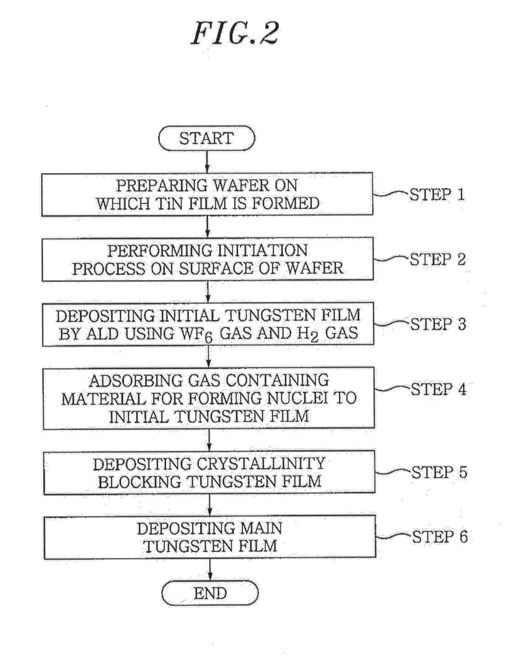
[0064]FIG. 2 is a flowchart of a film forming method in accordance with a first example of a first embodiment of the present invention. FIGS. 3A to 3F are cross-sectional views showing each process step.

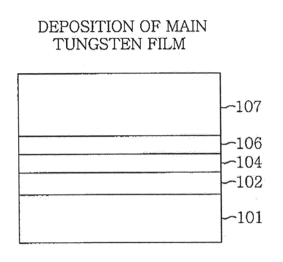
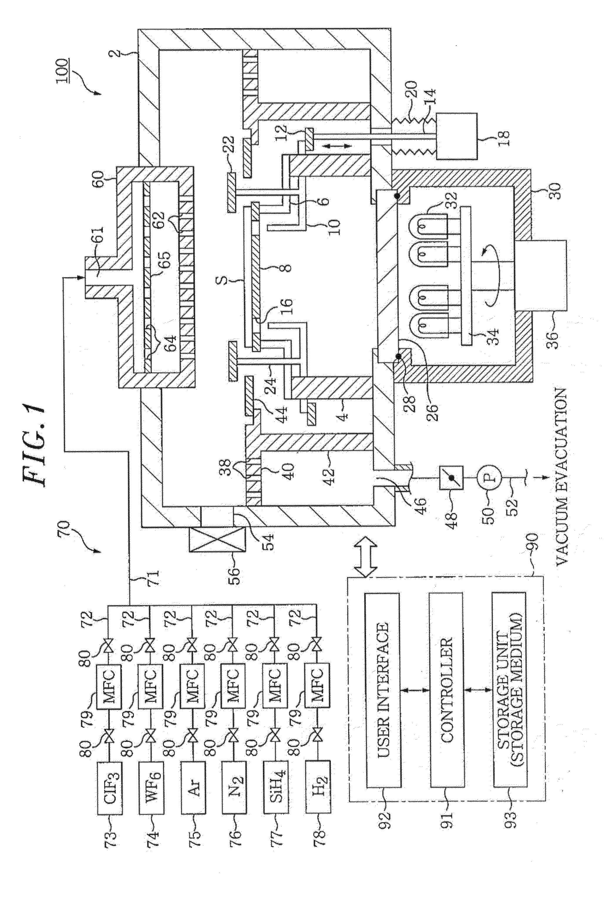
[0065]First of all, the wafer S in which a TiN film 102 is formed as a barrier layer of the surface on an interlayer insulating film 101 made of, e.g., SiO2 as shown in FIG. 3A is prepared and loaded into the processing chamber 2 (step 1). Further, holes (contact holes or via holes) have been formed actually in the interlayer insulating film 101, but the holes are omitted in FIGS. 3A to 3F for simplicity.

[0066]Then, a predetermined depressurized atmosphere is formed in the processing chamber 2, and while heating the wafer S through the mounting table 8 by the heating lamps 32 such that the temperature of the mounting table is 350 to 500° C., e.g., 410° C., a silane (SiH4) gas and a H2 gas or the like are introduced into the processing chamber 2, so that an initiation pro...

second example

[0151]FIG. 8 is a flowchart of a film forming method in accordance with a second example of the first embodiment of the present invention. This example is different from the first example in that the adsorption process of step 4 of the first example is not performed, and the other steps are performed in the same manner as the first example. That is, the wafer S having the structure of FIG. 3A is loaded into the processing chamber 2 (step 1), the initiation process is performed if necessary (step 2), the initial tungsten film is formed (step 3), the crystallinity blocking tungsten film is formed (step 5), and the main tungsten film is formed (step 6).

[0152]These steps 1, 2, 3, 5 and 6 are performed in the same manner as the first example. Further, as in the first example, it is preferable to perform the deposition of the main tungsten film discontinuously with the crystallinity blocking tungsten film. Also, it is preferable to set the time until the start of the deposition of the mai...

third example

[0154]FIG. 9 is a flowchart of a film forming method in accordance with a third example of the first embodiment of the present invention. This example is different from the first example in that the deposition of the crystallinity blocking tungsten film of step 5 of the first example is not performed, and the other steps are performed in the same manner as the first example. That is, the wafer S having the structure of FIG. 3A is loaded into the processing chamber 2 (step 1), the initiation process is performed if necessary (step 2), the initial tungsten film is formed (step 3), the adsorption process is performed (step 4), and the main tungsten film is formed (step 6).

[0155]These steps 1, 2, 3, 4 and 6 are performed in the same manner as the first example. Further, in the deposition of the main tungsten film, it is preferable to set the time until the start of the deposition of the main tungsten film after completion of the adsorption process in the range from 20 to 270 seconds. Ac...


PUM


Abstract

A tungsten film forming method for forming a tungsten film on a surface of a substrate while heating the substrate in a depressurized atmosphere in a processing chamber includes forming an initial tungsten film for tungsten nucleation on the surface of the substrate by alternately repeating a supply of WF6 gas which is raw material of tungsten and a supply of H2 gas which is a reducing gas in the processing chamber while performing a purge in the processing chamber between the supplies of the WF6 gas and the H2 gas and adsorbing a gas containing a material for nucleation onto a surface of the initial tungsten film. The film forming method further includes depositing a crystallinity blocking tungsten film for blocking crystallinity of the initial tungsten film by supplying the WF6 gas and the H2 gas into the processing chamber.

Description

CROSS-REFERENCE TO RELATED APPLICATION[0001]This application claims priority to Japanese Patent Application Nos. 2011-258117, 2012-051018, and 2012-183934 filed on Nov. 25, 2011, Mar. 7, 2012, and Aug. 23, 2012, respectively, the entire contents of which are incorporated herein by reference.FIELD OF THE INVENTION[0002]The present invention relates to a tungsten film forming method for forming a tungsten film on a substrate.BACKGROUND OF THE INVENTION[0003]In a process of manufacturing a semiconductor device, a tungsten (W) film is used to fill up recesses (via holes) between wirings or recesses (contact holes) for substrate contact.[0004]As a film forming method of the tungsten (W) film, physical vapor deposition (PVD) has been used in the past. However, since tungsten is metal with a high melting point and it is difficult to cope with high coverage due to the recent miniaturization of devices in the PVD, chemical vapor deposition (CVD) which can sufficiently cope with high coverage...

Claims


Application Information

Patent Timeline
Patent Type & Authority Applications(United States)
IPC IPC(8): H01L21/48
CPCH01L21/4814H01L21/28556H01L2221/1089H01L21/76876H01L21/76877H01L21/28562H01L21/205H01L21/31
Inventor SATOH, KOHICHI
Owner TOKYO ELECTRON LTD
Why Eureka
Try Eureka