Supercharge Your Innovation With Domain-Expert AI Agents!

Stress reduced cascoded CMOS output driver circuit

a driver circuit and cascode technology, applied in the direction of oscillator generators, digital storage, instruments, etc., can solve the problems of over-voltage stress across the device terminal, reliability issues, and tddb degradation of the devi

Active Publication Date: 2013-06-06
STMICROELECTRONICS INT NV
View PDF1 Cites 26 Cited by
  • Summary
  • Abstract
  • Description
  • Claims
  • Application Information

AI Technical Summary

Benefits of technology

The present invention provides an output driver circuit that includes four transistors, which are arranged in a common current path. The circuit receives different switching signals and reference voltages to produce an output signal. The transistors are arranged in a specific way to introduce delays and buffering to improve the performance of the circuit. The circuit has a compact size and can be used in various electronic devices. The technical effect of the invention is to provide a reliable and efficient output driver circuit for various electronic devices.

Problems solved by technology

The use of low voltage devices at high voltage results in over-voltage stress across the device terminals.
The over-voltage stress across the device terminals results in reliability issues (degradation) like Hot Carrier Injection (HCI), Bias Temperature Instability (BTI) and Time-Dependent Dielectric Breakdown (TDDB) degradation in the devices over time.
In such architectures the Vds stress (measured as the voltage difference between the drain and source terminals of the transistor) across the cascoded devices become very high during the transition, which leads to a very high HCI degradation in these cascoded devices.
However, in that approach ensuring the pulse width and synchronizing it with the output transition time becomes very complex, especially across the different PVT corners.

Method used


Image

  • Stress reduced cascoded CMOS output driver circuit
  • Stress reduced cascoded CMOS output driver circuit
  • Stress reduced cascoded CMOS output driver circuit

Examples


Embodiment Construction

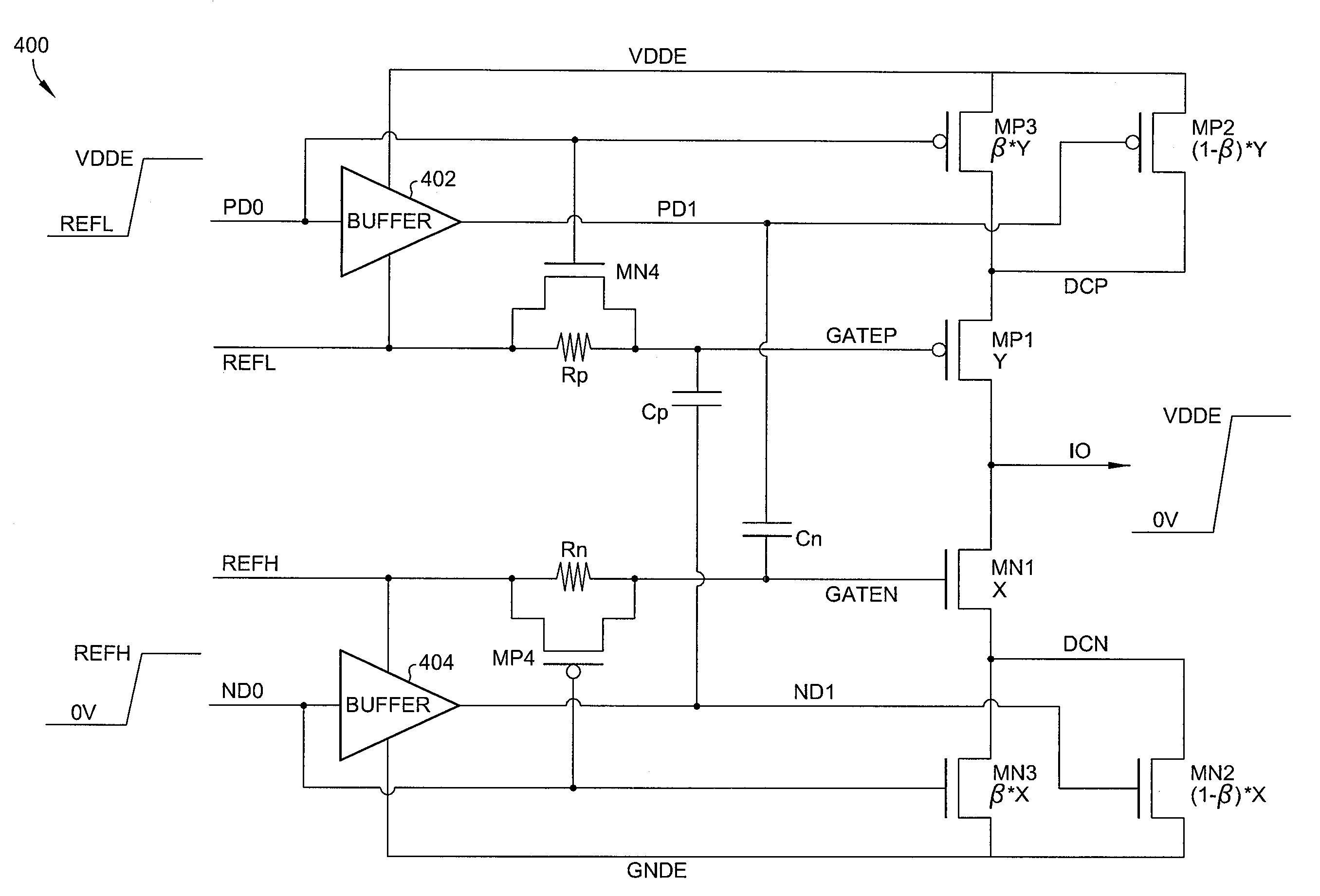
[0018]Referring now to FIG. 4, the circuit details of a new architecture of a cascoded output driver 400 are disclosed.

[0019]Output driver circuit 400 includes first (MP2), second (MP1), third (MN1), and fourth (MN2) transistors having a common current path, wherein a gate of the first transistor receives a first switching signal (PD0), a gate of the second transistor receives a first reference voltage (REFL), a gate of the third transistor receives a second reference voltage (REFH), and a gate of the fourth transistor receives a second switching signal (ND0), and wherein a first capacitor (Cn) is coupled between the gate of the first transistor and the gate of the third transistor, a second capacitor (Cp) is coupled between the gate of the second transistor and the gate of the fourth transistor, and an output signal (IO) is provided at a node coupling the second and third transistors. The first and second transistors comprise PMOS transistors, and the third and fourth transistors c...


PUM


Abstract

An output driver circuit includes first, second, third, and fourth transistors having a common current path, wherein a gate of the first transistor receives a first switching signal, a gate of the second transistor receives a first reference voltage, a gate of the third transistor receives a second reference voltage, and a gate of the fourth transistor receives a second switching signal, and wherein a first capacitor is coupled between the gate of the first transistor and the gate of the third transistor, a second capacitor is coupled between the gate of the second transistor and the gate of the fourth transistor, and an output signal is provided at a node coupling the second and third transistors.

Description

FIELD OF THE INVENTION[0001]The present invention relates to input and output driver circuits.BACKGROUND OF THE INVENTION[0002]As feature sizes of semiconductor technology continues to shrink, the need arises to design high voltage IO interfaces by using the low voltage devices. The use of low voltage devices at high voltage results in over-voltage stress across the device terminals. The over-voltage stress across the device terminals results in reliability issues (degradation) like Hot Carrier Injection (HCI), Bias Temperature Instability (BTI) and Time-Dependent Dielectric Breakdown (TDDB) degradation in the devices over time. To reduce the reliability degradation on such devices, design techniques are being used to reduce the over-voltage stress across the device terminals. The cascode technique is one of the most common techniques used to design the 2×VDD (VDDE) voltage level IO buffer by using VDD voltage level devices, in which the VDD level reference voltage (REFH and REFL) d...

Claims


Application Information

Patent Timeline
IPC IPC(8): H03B1/00
CPCG11C7/1057H03K3/02G11C7/1069
Inventor KUMAR, VINOD
Owner STMICROELECTRONICS INT NV
Features
  • R&D
  • Intellectual Property
  • Life Sciences
  • Materials
  • Tech Scout
  • Unparalleled Data Quality
  • Higher Quality Content
  • 60% Fewer Hallucinations
Learn More