
Display device

a technology of display device and pixel portion, which is applied in the direction of electrical apparatus construction details, instruments, optics, etc., can solve the problems of reducing the pitch between the protruding electrodes, complicated driving circuit for driving a pixel portion, and reducing the brightness of the display section, so as to avoid the increase in production lead time and avoid the increase in the frame width of the terminal section

Inactive Publication Date: 2013-06-06
PANASONIC INTELLECTUAL PROPERTY MANAGEMENT CO LTD
View PDF5 Cites 4 Cited by
  • Summary
  • Abstract
  • Description
  • Claims
  • Application Information

AI Technical Summary

Benefits of technology

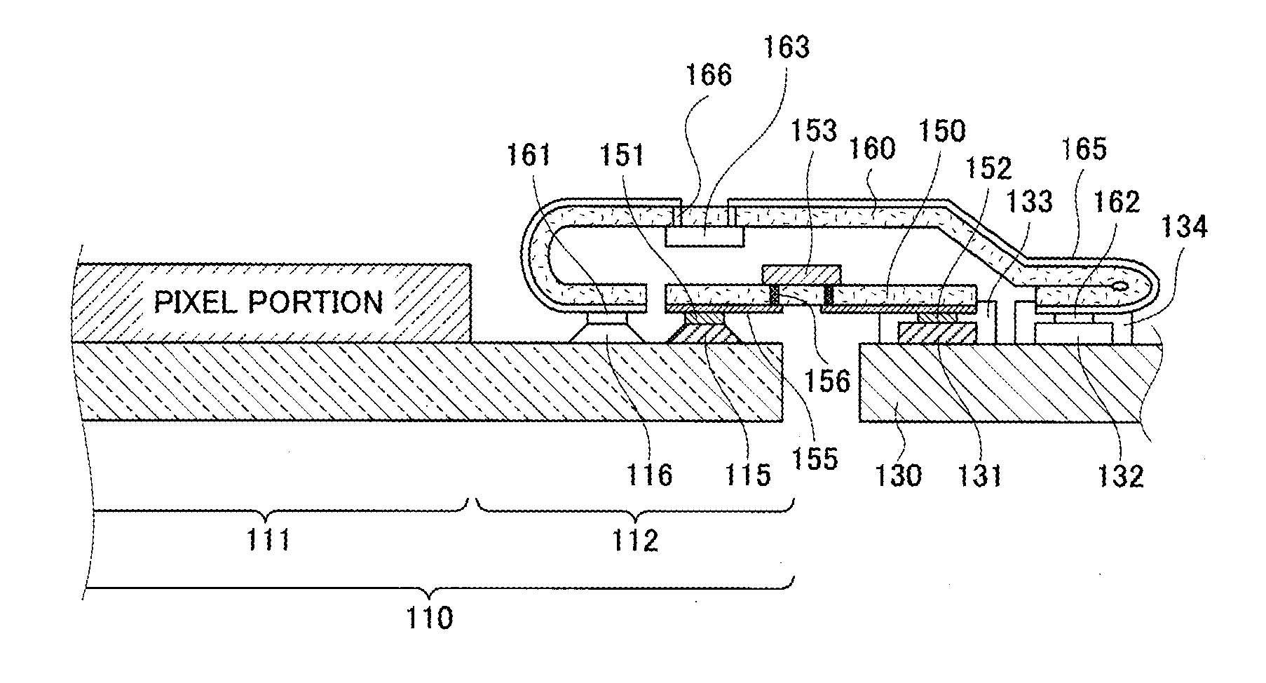
The invention allows two flexible printed boards to be connected to a terminal section in a single step, which avoids an increase in production lead time. Additionally, the invention avoids an increase in the frame width of the terminal section by arranging the first and second protruding electrodes next to each other.

Problems solved by technology

As the display section has higher resolution and smaller size, a pitch between the protruding electrodes disadvantageously decreases.
Moreover, variations in the amount of an applied organic EL material and degradation of the organic EL material cause an organic EL display device to emit light in varying amounts, leading to variations in luminance over the display section.
In order to eliminate variations in luminance, feedback processing on a voltage and a current is necessary, resulting in a complicated driving circuit for driving a pixel portion of the display section.
Accordingly, a pitch between the protruding electrodes disadvantageously decreases.

Method used


Image

  • Display device
  • Display device
  • Display device

Examples


embodiment

[0036]An embodiment according to the present invention will be described below with reference to the accompanying drawings.

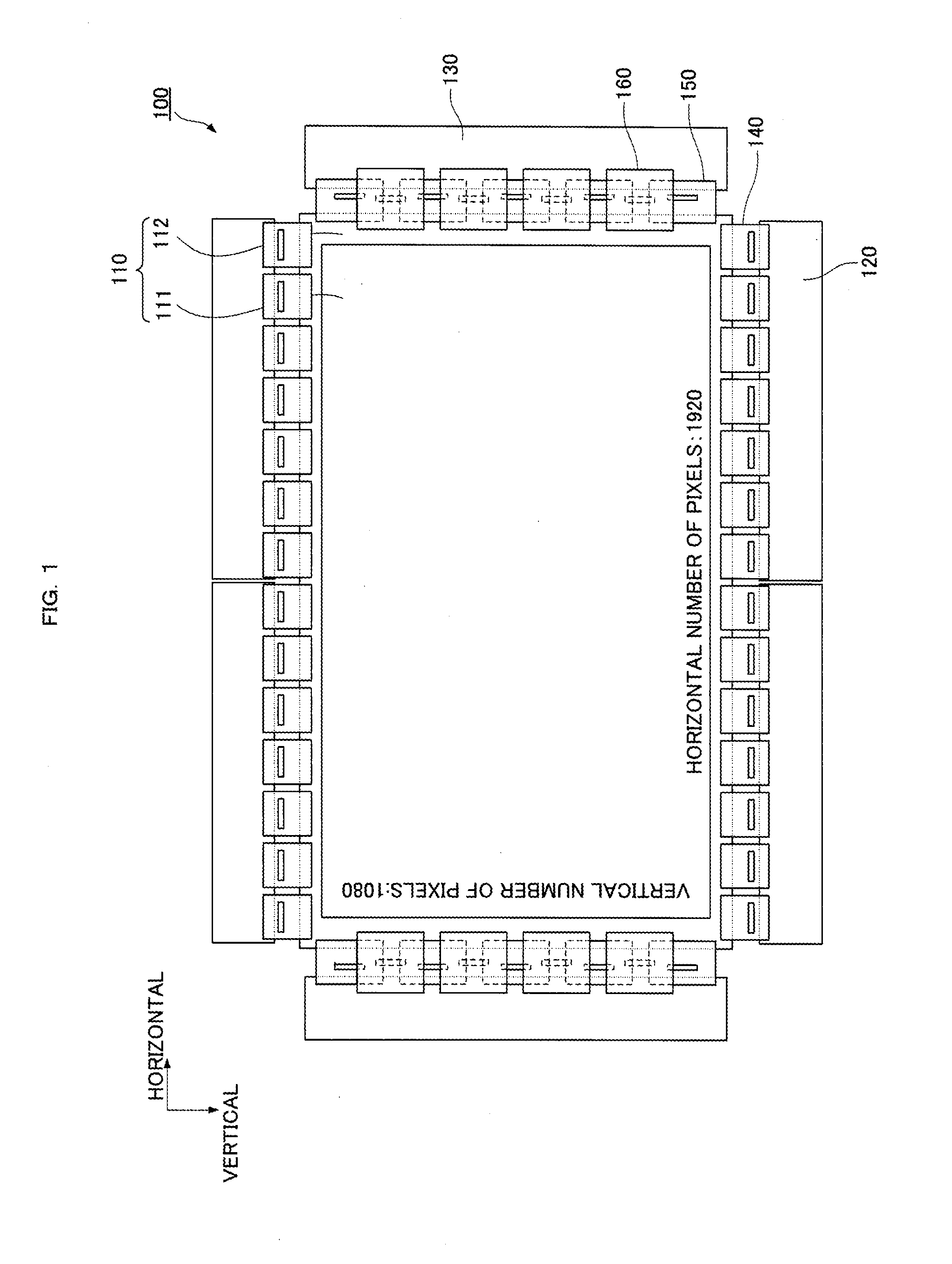
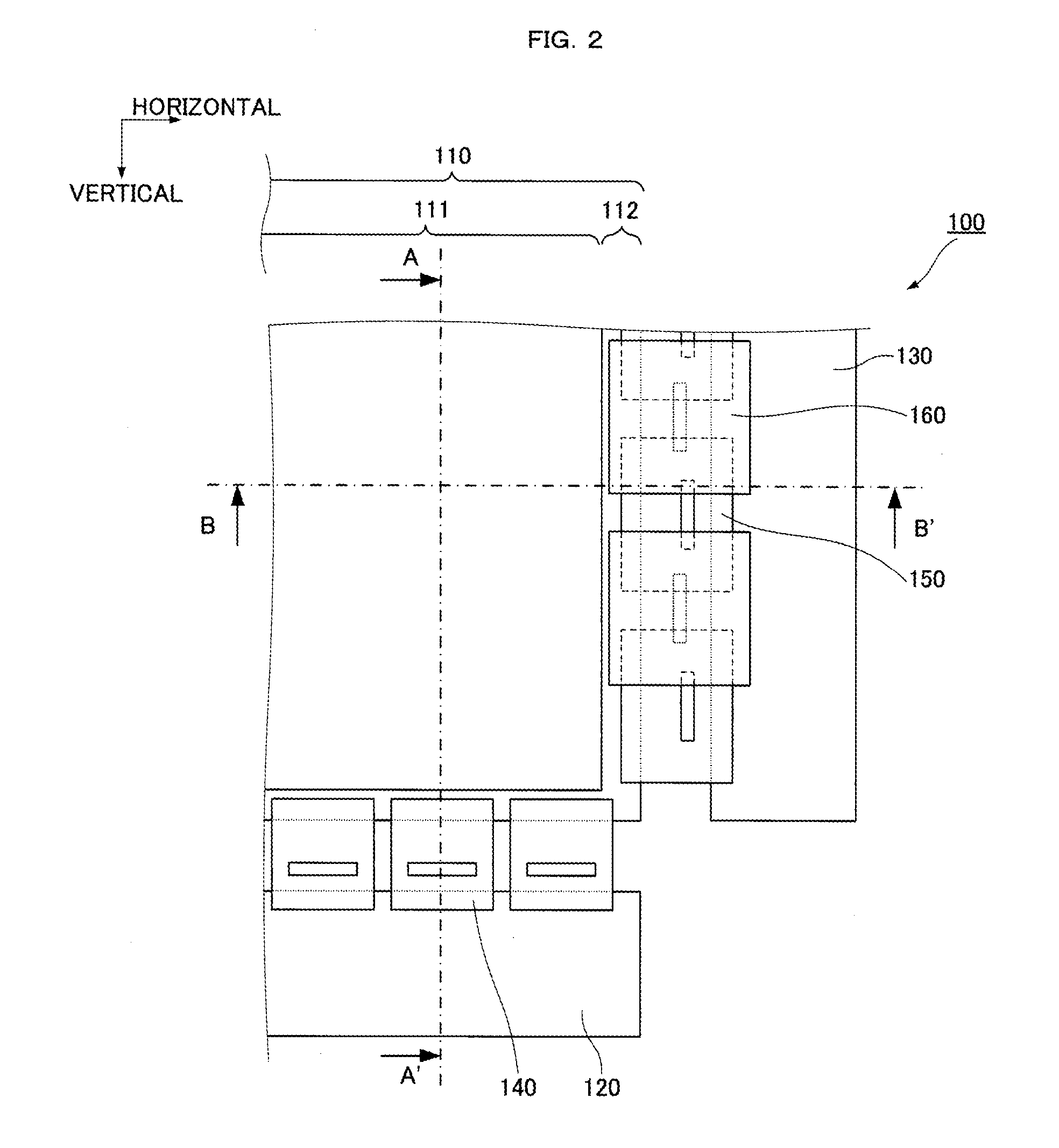
[0037]As illustrated in FIG. 1, in a display device 100 according to the present embodiment, external circuits 120 and 130 are disposed around a panel 110. The panel 110 includes a display section 111 that displays an image and a terminal section 112 formed around the display section 111. The external circuits 120 and 130 are glass epoxy multilayer boards that supply power, signals, and so on to the panel 110 to display images on the panel 110.

[0038]In this example, in the display device 100, the two external circuits 120 are disposed next to a horizontal part of the terminal section 112 on each of the upper and lower ends of the panel 110 with respect to the vertical direction. The external circuit 130 is disposed next to a vertical part of the terminal section 112 on each of the right and left ends of the panel 110 with respect to the horizontal direction. The...


PUM

PropertyMeasurementUnit
frequencyaaaaaaaaaa
pressureaaaaaaaaaa
widthaaaaaaaaaa

Abstract

In a display device (100), a row of protruding electrodes (115) and a row of protruding electrodes (116) are formed on the connecting surface of a terminal section (112), the row of the protruding electrodes (116) is disposed between the row of the protruding electrodes (115) and a display section (111), one end of a flexible printed board (150) is connected to the row of the protruding electrodes (115), one end of a flexible printed board (160) is connected to the row of the protruding electrodes (116), the row of the protruding electrodes (115) is adjacent to the row of the protruding electrodes (116), and the one end of the flexible printed board (150) and the one end of the flexible printed board (160) are opposed to each other.

Description

TECHNICAL FIELD[0001]The present invention relates to display devices such as a liquid crystal display device and an organic EL display device which can provide high-quality display with a smaller thickness and lower power consumption.BACKGROUND ART[0002]In recent years, display devices such as a liquid crystal display device and an organic EL display device have been developed which can provide high-quality display with a smaller thickness and lower power consumption. These display devices each include a display section that displays an image and a terminal section formed around the display section. The terminal section includes a plurality of protruding electrodes that are electrically connected to control lines for controlling the pixel portions of the display section. As the display section has higher resolution and smaller size, a pitch between the protruding electrodes disadvantageously decreases.[0003]Moreover, variations in the amount of an applied organic EL material and de...

Claims


Application Information

Patent Timeline
Patent Type & Authority Applications(United States)
IPC IPC(8): H05K7/00H05K13/00
CPCG02F1/13452H05K1/147H05K3/323H05K3/361H05K2201/055H05K7/00Y10T29/49124H01L2924/0002H05K13/00H05K2201/09445H05K2201/045H01L2924/00
Inventor NOBORI, KAZUHIRO
Owner PANASONIC INTELLECTUAL PROPERTY MANAGEMENT CO LTD
Learn More