Light emitting diode with multiple transparent conductive layers and method for manufacturing the same

a technology of transparent conductive layer and light-emitting diodes, which is applied in the direction of semiconductor/solid-state device manufacturing, electrical apparatus, semiconductor devices, etc., can solve the problems of poor electrical properties of transparent conductive layers, relatively short manufacturing time, and relative high electrical properties

Inactive Publication Date: 2013-06-13
ADVANCED OPTOELECTRONICS TECH
View PDF8 Cites 0 Cited by
  • Summary
  • Abstract
  • Description
  • Claims
  • Application Information

AI Technical Summary

Benefits of technology

[0005]The transparent conductive layer is required to have a relatively high electrical property and a relatively short manufacturing time. The electrical property of the transparent conductive layer varies along with different parameters for forming the transparent conductive layer. The higher the density of the transparent conductive layer is, the better the electrical property but the longer the manufacturing time of the transparent conductive layer is required. In contrast, the lower the density of the transparent conductive layer is, the shorter the manufacturing time required, but the poorer the electrical property of the transparent conductive layer is.

Problems solved by technology

The transparent conductive layer is required to have a relatively high electrical property and a relatively short manufacturing time.
In contrast, the lower the density of the transparent conductive layer is, the shorter the manufacturing time required, but the poorer the electrical property of the transparent conductive layer is.

Method used


Image

  • Light emitting diode with multiple transparent conductive layers and method for manufacturing the same
  • Light emitting diode with multiple transparent conductive layers and method for manufacturing the same
  • Light emitting diode with multiple transparent conductive layers and method for manufacturing the same

Examples


Embodiment Construction

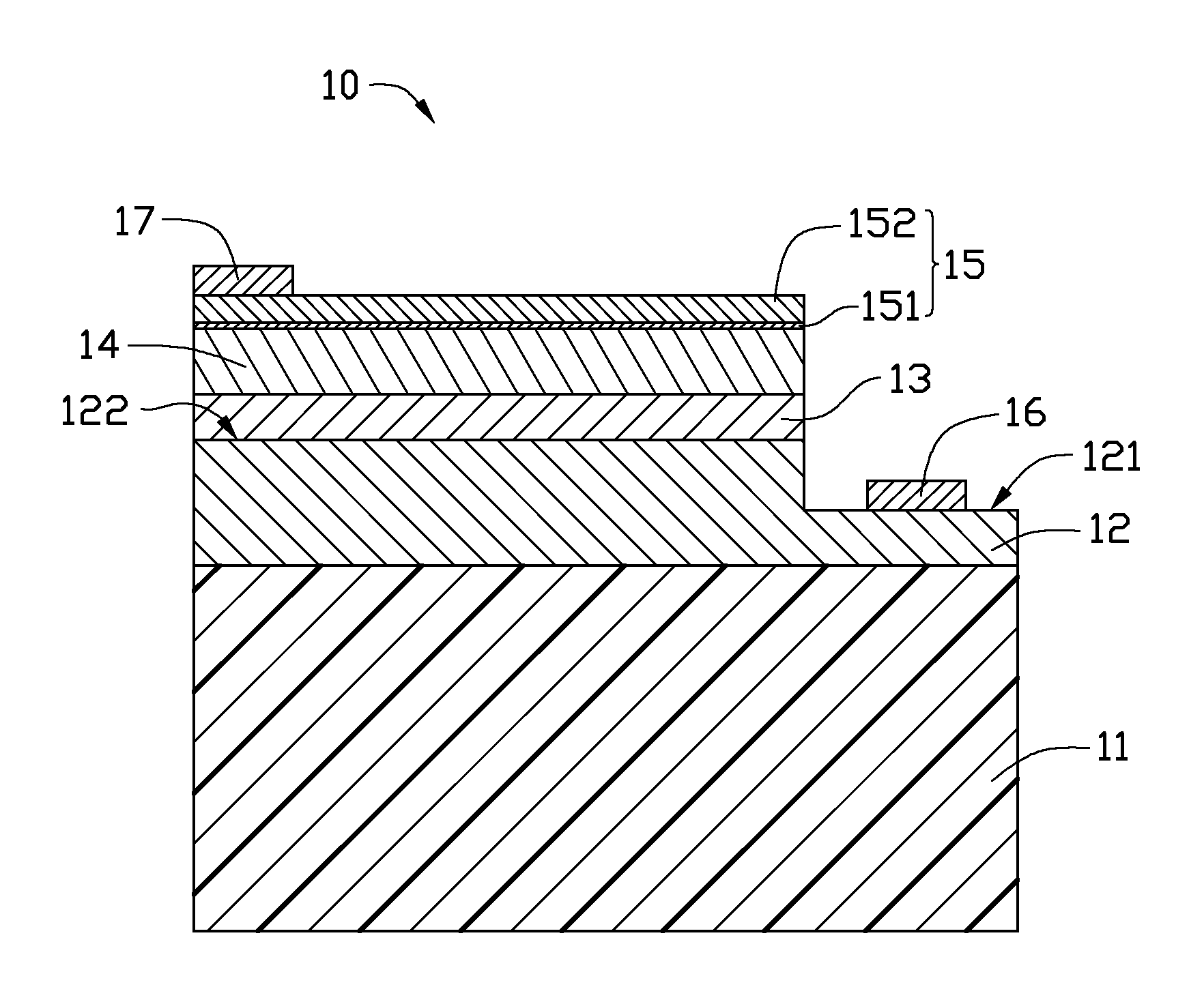
[0010]Referring to FIG. 1, a light emitting diode 10 in accordance with one embodiment is provided. The light emitting diode 10 includes a substrate 11, a light emitting structure, a transparent conductive layer 15 formed on the light emitting structure, a first electrode 16, and a second electrode 17 having an opposite polarity with respect to the first electrode 16. In this embodiment, the light emitting structure includes a first-type semiconductor layer 12, an active layer 13 and a second-type semiconductor layer 14. The transparent conductive layer 15 is transparent to light and conductive to electricity. When a bias is applied to the first and second electrodes 16, 17, electron holes and electrons flow from the first-type semiconductor layer 12 and the second-type semiconductor layer 14 to recombine at the active layer 13, whereby light is emitted from the active layer 13.

[0011]The substrate 11 is dielectric. The substrate 11 can be sapphire (α-Al2O3) substrate, silicon carbid...


PUM


Abstract

An LED includes a first semiconductor layer, a second semiconductor layer, an active layer, a first transparent conductive layer, and a second transparent conductive layer. The first transparent conductive layer is formed on the second semiconductor layer. The second transparent conductive layer is formed on the first transparent conductive layer. The thickness of the first transparent conductive layer is less than that of the second transparent conductive layer. The density of the first transparent conductive layer is larger than that of the second transparent conductive layer. The disclosure further includes a method for manufacturing the LED.

Description

BACKGROUND[0001]1. Technical Field[0002]The disclosure relates to light emitting diodes, and particularly to a light emitting diode with multiple transparent conductive layers and a method for manufacturing the light emitting diode.[0003]2. Description of the Related Art[0004]A conventional light emitting diode (LED) includes a substrate, a light emitting structure having an N-type semiconductor layer, an active layer and a P-type semiconductor layer formed on the substrate in sequence, and two electrodes (i.e., N-type and P-type electrodes) respectively connected to the N-type and P-type semiconductor layers. To obtain an even current distribution in the semiconductor layers while do not lower the light extraction efficiency, a transparent conductive layer which is made of indium tin oxide (ITO) is formed on the light emitting structure.[0005]The transparent conductive layer is required to have a relatively high electrical property and a relatively short manufacturing time. The ele...

Claims


Application Information

Patent Timeline
Patent Type & Authority Applications(United States)
IPC IPC(8): H01L33/42H01L33/06
CPCH01L33/42H01L2933/0016
Inventor SHEN, CHIA-HUIHUNG, TZU-CHIEN
Owner ADVANCED OPTOELECTRONICS TECH
Why Eureka
Try Eureka