Capacitive bonding structure for electronic devices

a technology of capacitor and electronic device, applied in the direction of semiconductor device, semiconductor/solid-state device details, electrical apparatus, etc., can solve the problems of parasitical inductance, insertion loss, and critical quality of such electronic components, and achieve low insertion loss, good electrical connection, and high operating frequency

Inactive Publication Date: 2013-06-13
NAT TAIPEI UNIV OF TECH
View PDF9 Cites 0 Cited by
  • Summary
  • Abstract
  • Description
  • Claims
  • Application Information

AI Technical Summary

Benefits of technology

[0011]The objective of the invention is to present a bonding structure for high-frequency electronic devices, employing a capacitor to provide connecti

Problems solved by technology

As most wireless products are made of various high-frequency active/passive electronic components, the quality of such electronic components becomes critical.
However, the insertion loss caused by the parasitical inductance, which is induced by the bonding wire 150a of approximate 60 mil in length, becomes severe when the bonding structure 100a is operated at high frequencies.
However, due to the oversize problem about the width of the aluminum strip in the bonding structure 100b of the conventional ribbon-bonding

Method used


Image

  • Capacitive bonding structure for electronic devices
  • Capacitive bonding structure for electronic devices
  • Capacitive bonding structure for electronic devices

Examples


Embodiment Construction

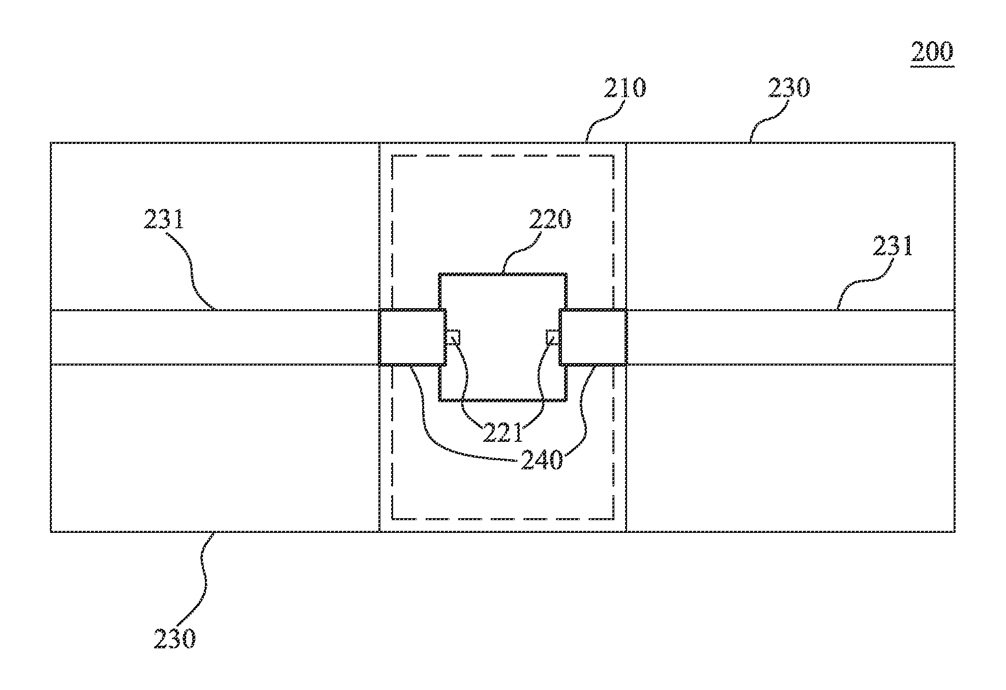
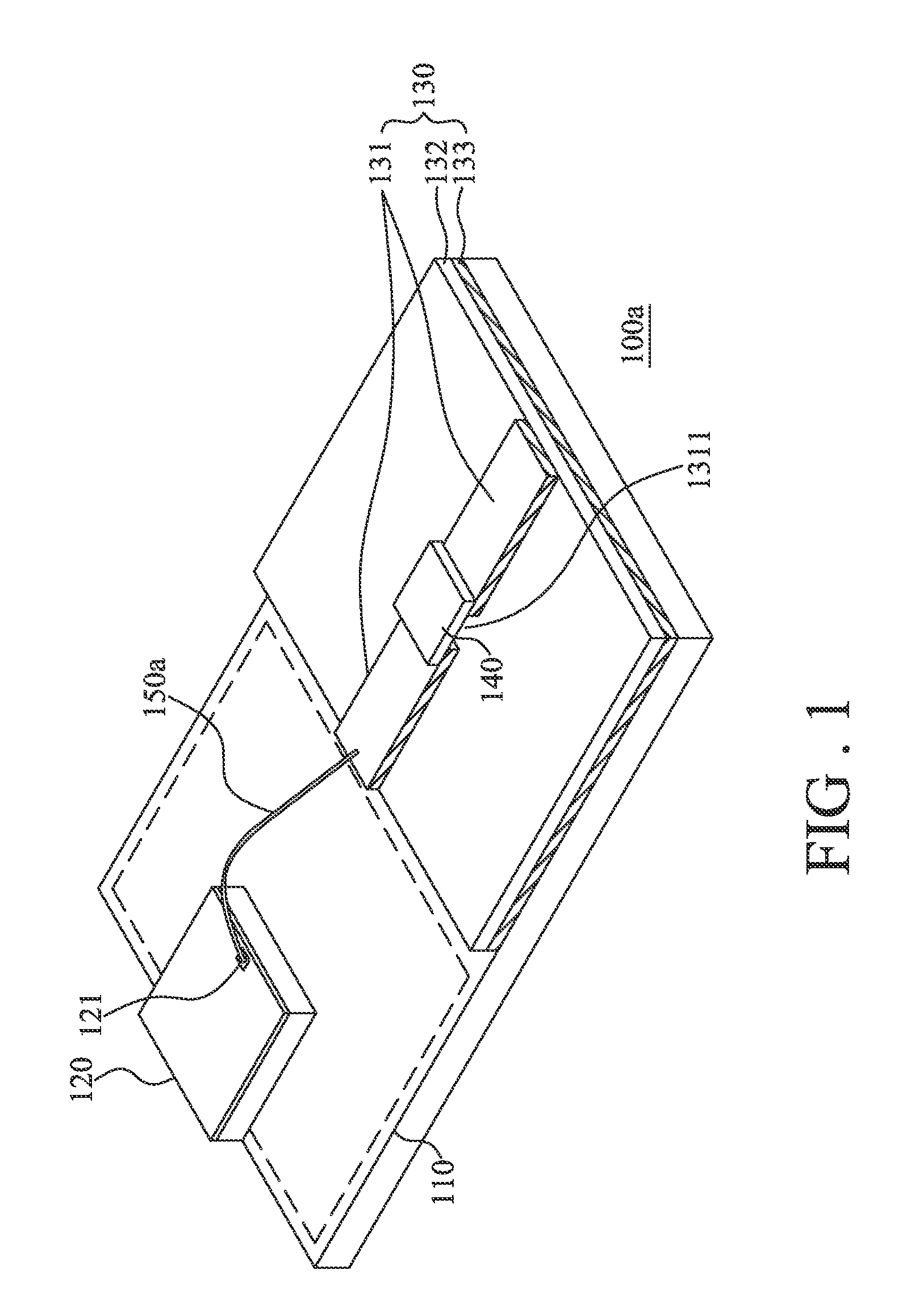
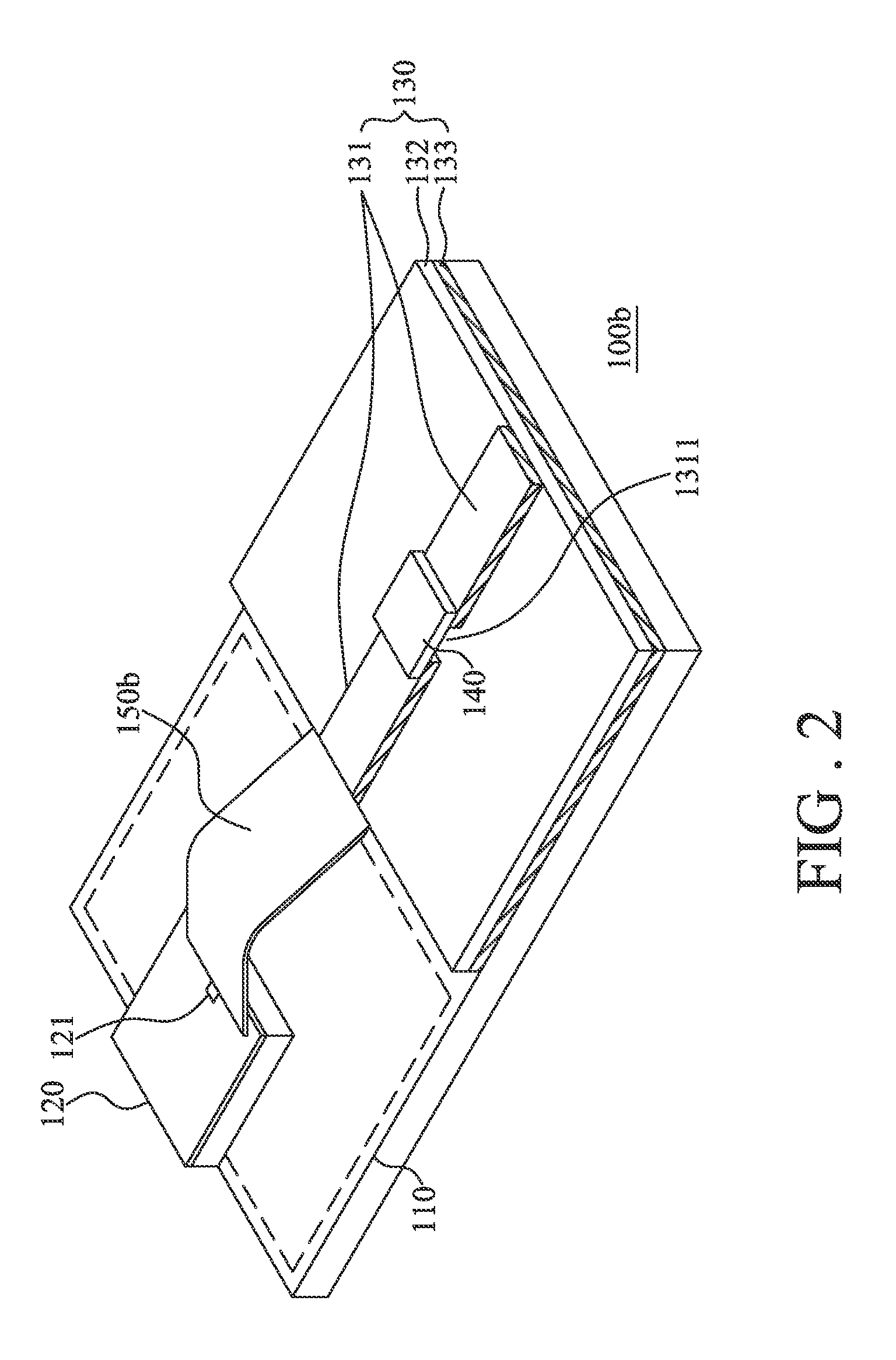
[0026]In the following detailed description of the preferred embodiments, references are made to the accompanying drawings which form a part hereof, and in which the specific embodiments likely to be the realization of the present invention are illustrated. In this regard, terminologies related to direction, such as “top,”“bottom,”“front,”“back,” etc., are used to refer to the orientations of the objects described in the figure(s). The constituents of the present invention can be positioned in a number of different orientations. As such, the terminologies related to direction are used for the purpose of illustration and are in no way of limiting the present invention. On the other hand, the drawings are only schematic plots and the sizes of the constituents may he exaggerated for the purpose of clarity. It is to be understood that other embodiments may be utilized with changes likely made in the structure of the present invention, but do not depart from the scope of the present inve...


PUM


Abstract

A bonding structure is applied to electrically connect a chip and a circuit board, such as a micro-strip line, for signal transmission between each other. The bonding structure includes a metallic plate and a capacitor. The chip and the micro-strip line are placed on the metallic plate but do not overlap or contact with each other. In particular, the capacitor is used to connect a signal pad of the chip and a signal line of the micro-strip line for signal transmission at high frequencies.

Description

BACKGROUND OF THE INVENTION[0001](1) Field of the Invention[0002]This invention relates to a bonding structure, and particularly to a capacitive bonding structure for high-frequency electronic devices.[0003](2) Description of the Prior Art[0004]Recently, following the advances in wireless communications technology, the services provided by wireless communications and their close connection to the Internet have made the market of wireless communications booming nowadays. As most wireless products are made of various high-frequency active / passive electronic components, the quality of such electronic components becomes critical. To ensure the quality of these wireless products, the fabrication of these high-frequency electronic components becomes very important.[0005]In order to meet the requirements, a device chip, usually an integrated circuit (IC) chip, is required to be connected to a signal line of a planar transmission line such as a micro-strip line. Conventional techniques to c...

Claims


Application Information

Patent Timeline
IPC IPC(8): H03H7/38
CPCH01L2224/48091H01L2924/19104H01L2224/48227H01L2924/00014H01L2224/45015H01L2224/13116H01L2224/48011H01L2924/3011H01L2223/6627H01L23/66H01L23/642H01L2224/37124H01L2224/16225H01L24/01H01L2224/40227H01L2924/30107H01L2924/00H01L2224/45099H01L2924/20752H01L2924/00015H01L2924/20651H01L2924/0105H01L2224/84801
Inventor LI, ERIC S.SHIAO, YU-SHAOCHIUEH, TZI-HONGCHEN, SHU-YANG
Owner NAT TAIPEI UNIV OF TECH
Why Eureka
Try Eureka