Perforation patterned electrical interconnects

a technology of perforation and electrical interconnection, which is applied in the direction of electrical apparatus, semiconductor devices, semiconductor/solid-state device details, etc., can solve the problem of difficult to create a manufacturing process that achieves low contact resistan

Inactive Publication Date: 2013-06-20
ITN ENERGY SYST INC
View PDF0 Cites 4 Cited by
  • Summary
  • Abstract
  • Description
  • Claims
  • Application Information

AI Technical Summary

Problems solved by technology

Using current techniques, it may be difficult to create a manufacturing process that achieves low contact resistance while also allowing for a high manufacturing tolerance.

Method used


Image

  • Perforation patterned electrical interconnects
  • Perforation patterned electrical interconnects
  • Perforation patterned electrical interconnects

Examples


Embodiment Construction

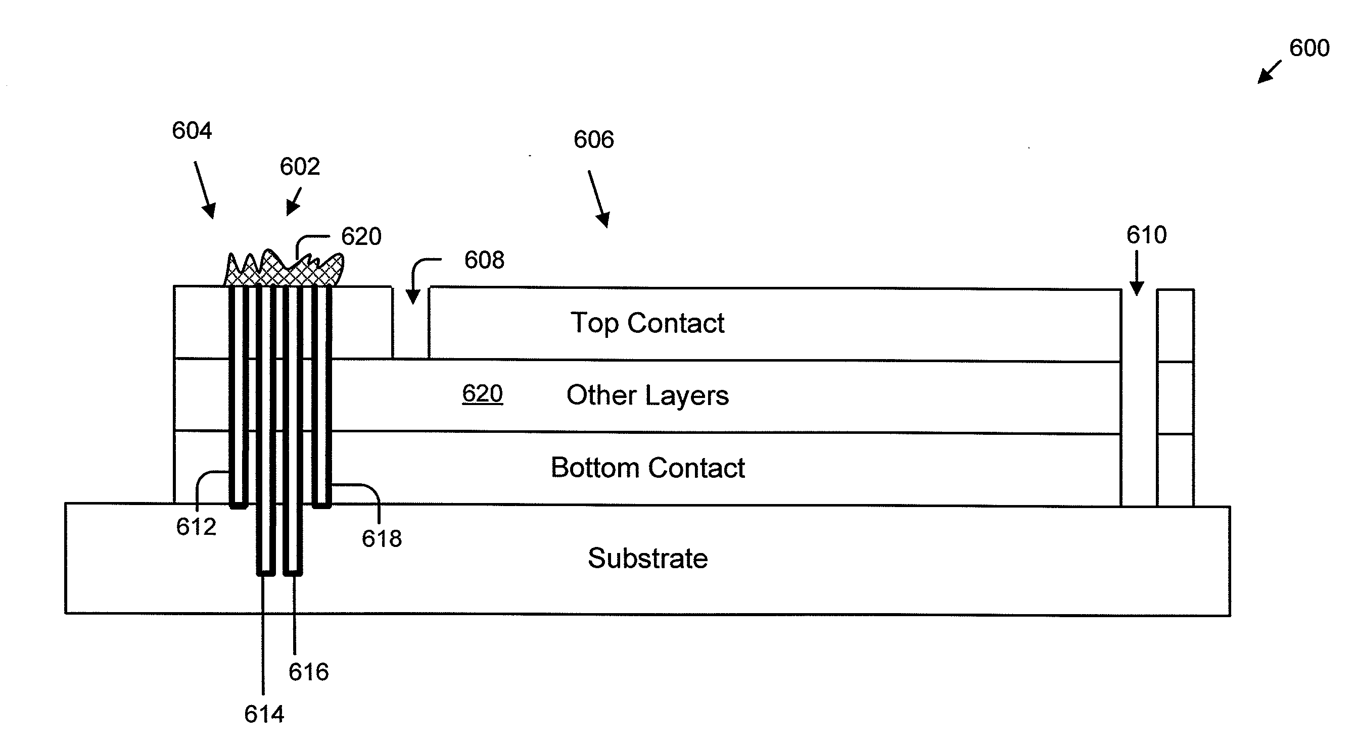
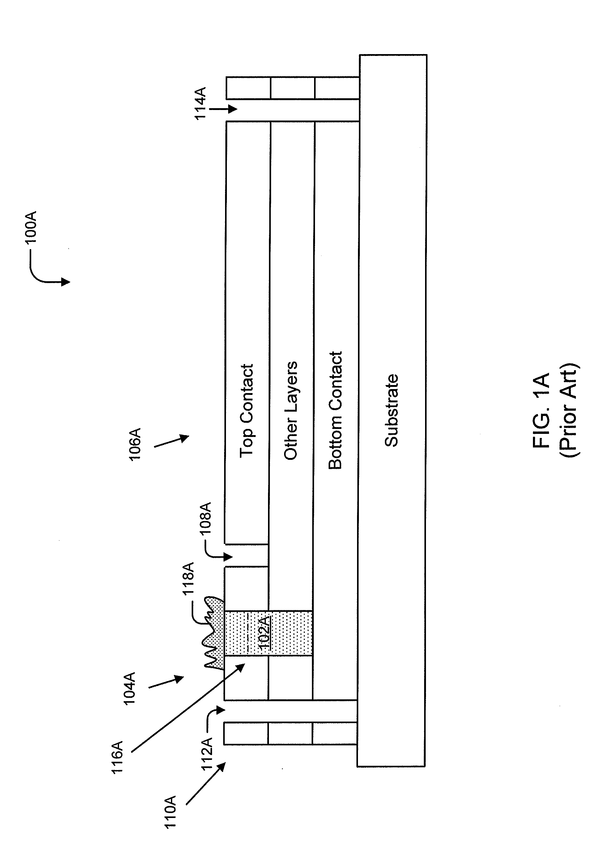
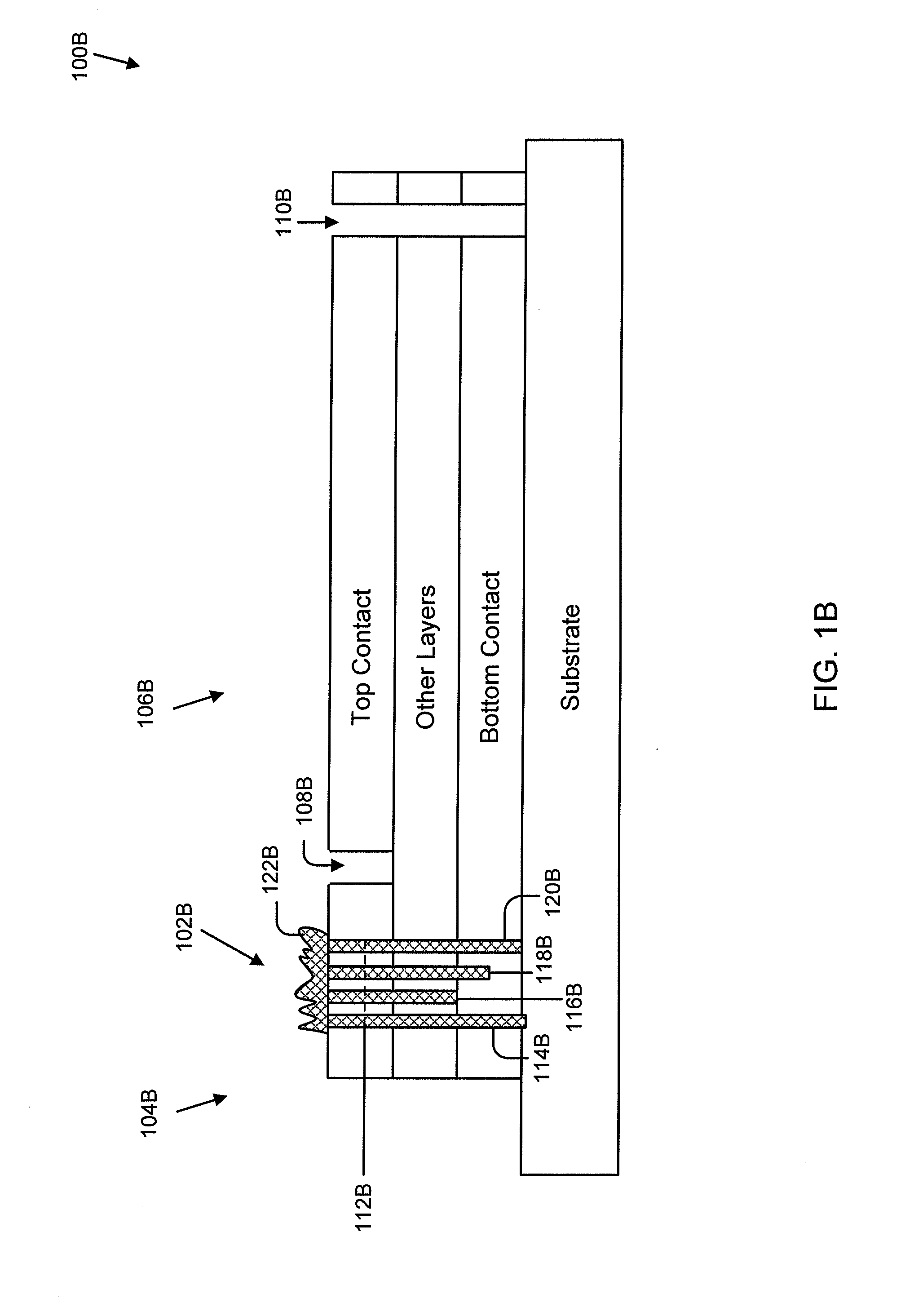
[0018]A device may have multiple layers that may be electrically coupled together. It may be desirous to electrically couple the layers together using electrically conductive interconnects. To accomplish this, one may penetrate the multiple layered device with one or more electrically conductive interconnects.

[0019]For example, FIG. 1A illustrates a vertical cross-section of an embodiment of a thin film solid state device 100A that includes the use of an electrically conductive interconnect 102A. In the embodiment 100A, the device has a substrate, a bottom contact, other layers, and a top contact. In embodiments, the top contact may be divided into three portions. A first top contact layer portion 104A may be electrically isolated from a second top contact layer portion 106A by an etch 108A. Additionally, the first top contact layer portion 104A may be electrically isolated from a third top contact layer portion 110A by an etch 112A. Other etches, such as etch 114A may further segme...


PUM


Abstract

This disclosure describes systems and methods for increasing the usable surface area of electrical contacts within a device, such as a thin film solid state device, through the implementation of electrically conductive interconnects. Embodiments described herein include the use of a plurality of electrically conductive interconnects that penetrate through a top contact layer, through one or more multiple layers, and into a bottom contact layer. The plurality of conductive interconnects may form horizontal and vertical cross-sectional patterns. The use of lasers to form the plurality of electrically conductive interconnects from reflowed layer material further aids in the manufacturing process of a device.

Description

RELATED APPLICATIONS[0001]This application claims the benefit of U.S. Provisional Application No. 61 / 576,246, filed Dec. 15, 2011, which application is hereby incorporated by reference.GOVERNMENT LICENSE RIGHTS[0002]This invention was made with government support under grant number DE-AR0000019 awarded by the Department of Energy. The government has certain rights in the invention.INTRODUCTION[0003]Solid state batteries, solar cells, and semiconductor devices may use electrically conductive interconnects. In conjunction with these devices, electrically conductive interconnects may be used in thin film, solid state, electrochemical, and other electrical integration schemes. Of these electrical integration schemes, solid state devices have the advantage of being composed of solid materials. This composition allows solid state devices to operate in a variety of conditions. These conditions may include varied physical orientations and a wide temperature range. Additionally, electrochemi...

Claims


Application Information

Patent Timeline
Patent Type & Authority Applications(United States)
IPC IPC(8): H01L23/48
CPCH01L23/481H01L31/022425H01L23/5226Y02E10/50H01L2924/0002H01L31/0465H01L2924/00H01L31/02008
Inventor FREY, JONATHAN
Owner ITN ENERGY SYST INC
Why Eureka
Try Eureka