Chip resistor and method of manufacturing the same

a technology of chip resistor and manufacturing method, which is applied in the direction of resistor, resistor details, resistor manufacturing, etc., can solve the problems of high material expense of chip resistor, increase manufacturing cost, and increase mass production of chip resistor, and achieve low resistance and small temperature coefficient of resistance (tcr).

Active Publication Date: 2013-06-20
SAMSUNG ELECTRO MECHANICS CO LTD
View PDF9 Cites 23 Cited by
  • Summary
  • Abstract
  • Description
  • Claims
  • Application Information

AI Technical Summary

Benefits of technology

[0010]An aspect of the present invention provides a chip resistor having relatively low resistance and a relatively small temperature coefficient of resistance (TCR), and a method of manufacturing the same.

Problems solved by technology

However, since the plate-type metal method requires a metal plate and a mold according to the required resistance range and size of the plate-type metal material, manufacturing costs are increased when various types of products are manufactured, and it is difficult to mass-produce chip resistors, as compared with the thick film method, and material expense is high in a chip resistor due to high use and unit costs of raw materials.
When this method is used, there is a limit in obtaining low resistance of 50 mΩ or less and a TCR of 500 ppm / K or less.

Method used


Image

  • Chip resistor and method of manufacturing the same
  • Chip resistor and method of manufacturing the same
  • Chip resistor and method of manufacturing the same

Examples


Embodiment Construction

[0062]Embodiments of the present invention will now be described in detail with reference to the accompanying drawings.

[0063]The embodiments of the present invention may be modified in many different forms and the scope of the invention should not be limited to the embodiments set forth herein.

[0064]Rather, these embodiments are provided so that this disclosure will be thorough and complete, and will fully convey the concept of the invention to those skilled in the art.

[0065]In the drawings, the shapes and dimensions may be exaggerated for clarity, and the same reference numerals will be used throughout to designate the same or like components.

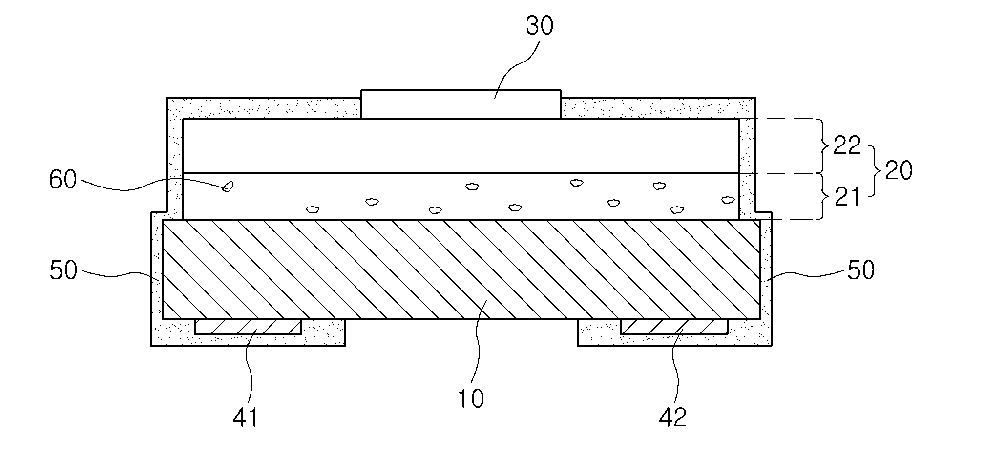
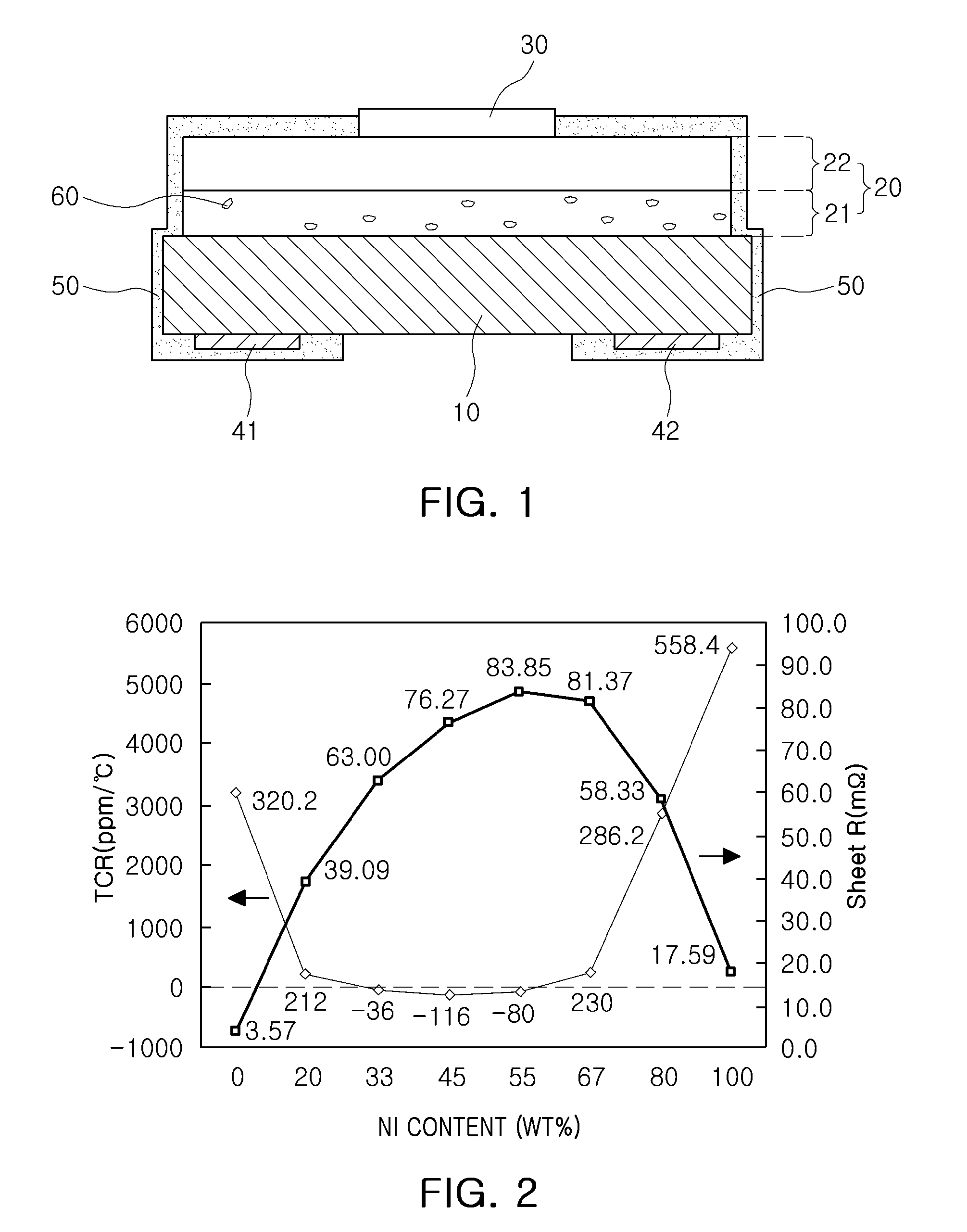
[0066]FIG. 1 is a cross-sectional view of a chip resistor according to an embodiment of the present invention.

[0067]Referring to FIG. 1, the chip resistor according to an embodiment of the present invention may include a ceramic substrate 10; and a resistance layer 20 formed on the ceramic substrate 10.

[0068]The ceramic substrate 10 may refer ...


PUM

PropertyMeasurementUnit
thicknessaaaaaaaaaa
thicknessaaaaaaaaaa
total thicknessaaaaaaaaaa

Abstract

There is provided a chip resistor including a ceramic substrate; a first resistance layer formed on the ceramic substrate and including a first conductive metal and a first glass; and a second resistance layer formed on the first resistance layer, including a second conductive metal and a second glass, and having a smaller content of glass than the first resistance layer, thereby obtaining relatively low resistance and a relatively small temperature coefficient of resistance (TCR).

Description

CROSS-REFERENCE TO RELATED APPLICATIONS[0001]This application claims the priority of Korean Patent Application No. 10-2011-0137250 filed on Dec. 19, 2011, in the Korean Intellectual Property Office, the disclosure of which is incorporated herein by reference.BACKGROUND OF THE INVENTION[0002]1. Field of the Invention[0003]The present invention relates to a chip resistor and a method of manufacturing the same.[0004]2. Description of the Related Art[0005]According to the related art, a resistor having low resistance ranging from 50 mΩ to 1Ω is manufactured through a thick film method. A resistor electrode is formed of a silver (Ag)-palladium (Pd) paste and a side electrode portion is formed of an Ag paste.[0006]By changing the pattern sizes of the resistor electrode and the side electrode portion and adjusting Pd content of the Ag—Pd paste of the resistor electrode, a temperature coefficient of resistance (TCR) is adjusted.[0007]In a plate-type metal method, resistance is adjusted by u...

Claims


Application Information

Patent Timeline
Patent Type & Authority Applications(United States)
IPC IPC(8): H01C1/012H01C17/00
CPCH01C17/06526Y10T29/49082H01C17/065H01C7/18H01C1/14H01C7/00
Inventor PARK, JANG HOKIM, YOUNG KEYSUH, KI WONYUN, JANG SEOKHAN, JIN MANKIM, SUNG JUN
Owner SAMSUNG ELECTRO MECHANICS CO LTD
Why Eureka
Try Eureka