Method of manufacturing semiconductor device

Inactive Publication Date: 2013-06-20
NITTO DENKO CORP
View PDF4 Cites 11 Cited by
  • Summary
  • Abstract
  • Description
  • Claims
  • Application Information

AI Technical Summary

Benefits of technology

[0014]According to the method of manufacturing a semiconductor device of the present invention, a plurality of semiconductor chips are embedded in the thermosetting resin layer (step D). Therefore, the thermosetting resin layer can be used as a sealing material to seal the semiconductor chips. Because the semiconductor chips are embedded directly in the thermosetting resin layer, a step of temporarily fixing the semiconductor chips and a sheet to temporarily fix the semiconductor chips are not necessary. As a result, the pro

Problems solved by technology

In addition, a large number of terminals are formed in the semiconductor chip region of a BGA (Ball Grid Array) package, and the region where other elements can be formed is limited.
Under such circumstances, if the miniaturization of semiconductor devices and the

Method used


Image

  • Method of manufacturing semiconductor device
  • Method of manufacturing semiconductor device
  • Method of manufacturing semiconductor device

Examples


second embodiment

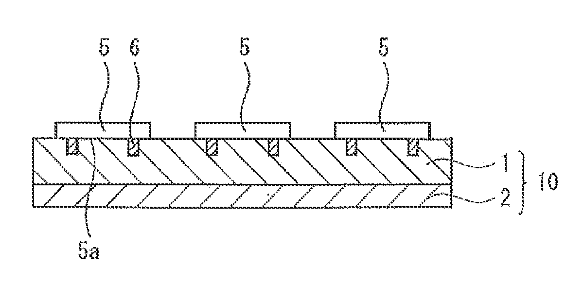
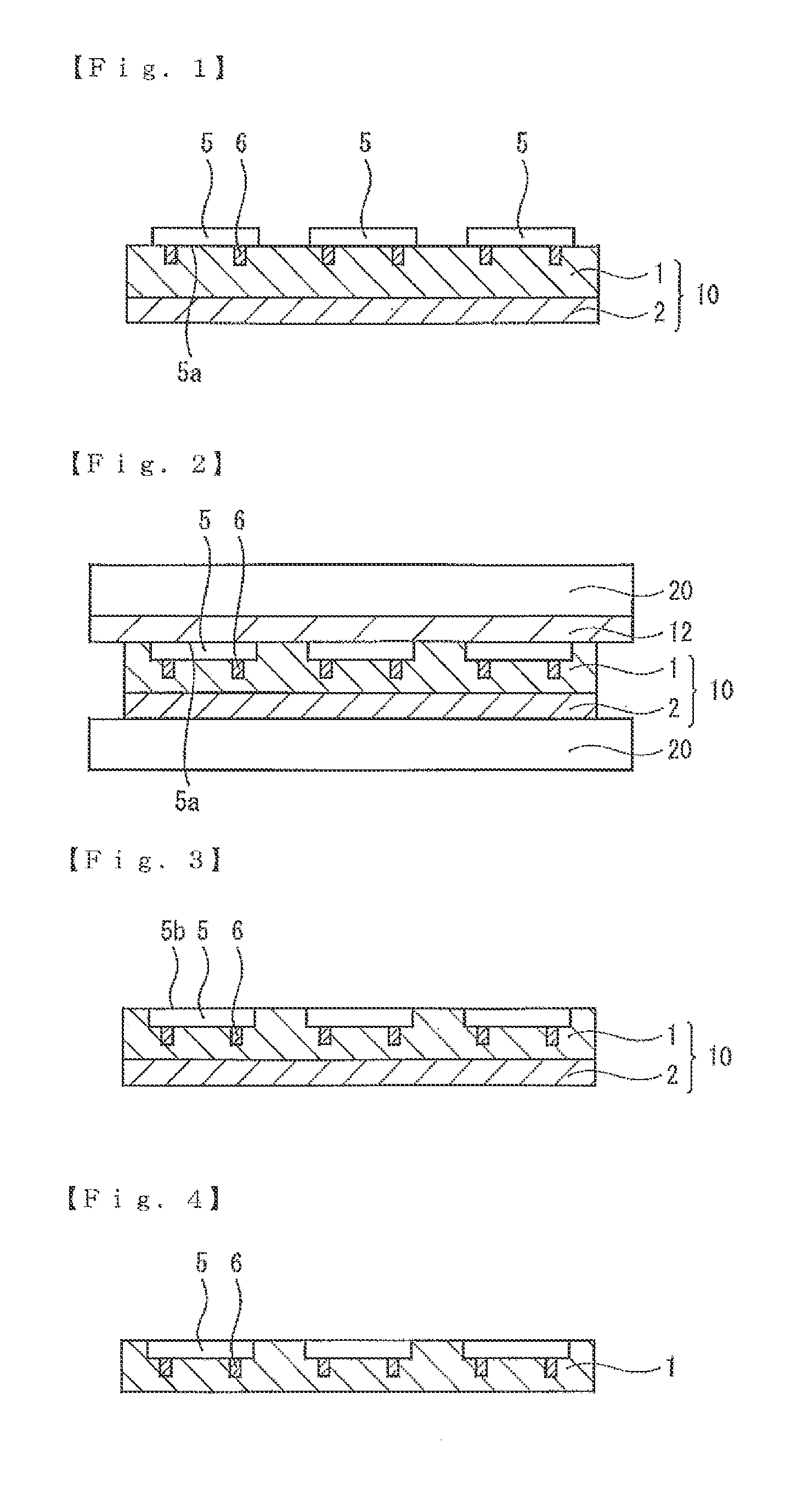
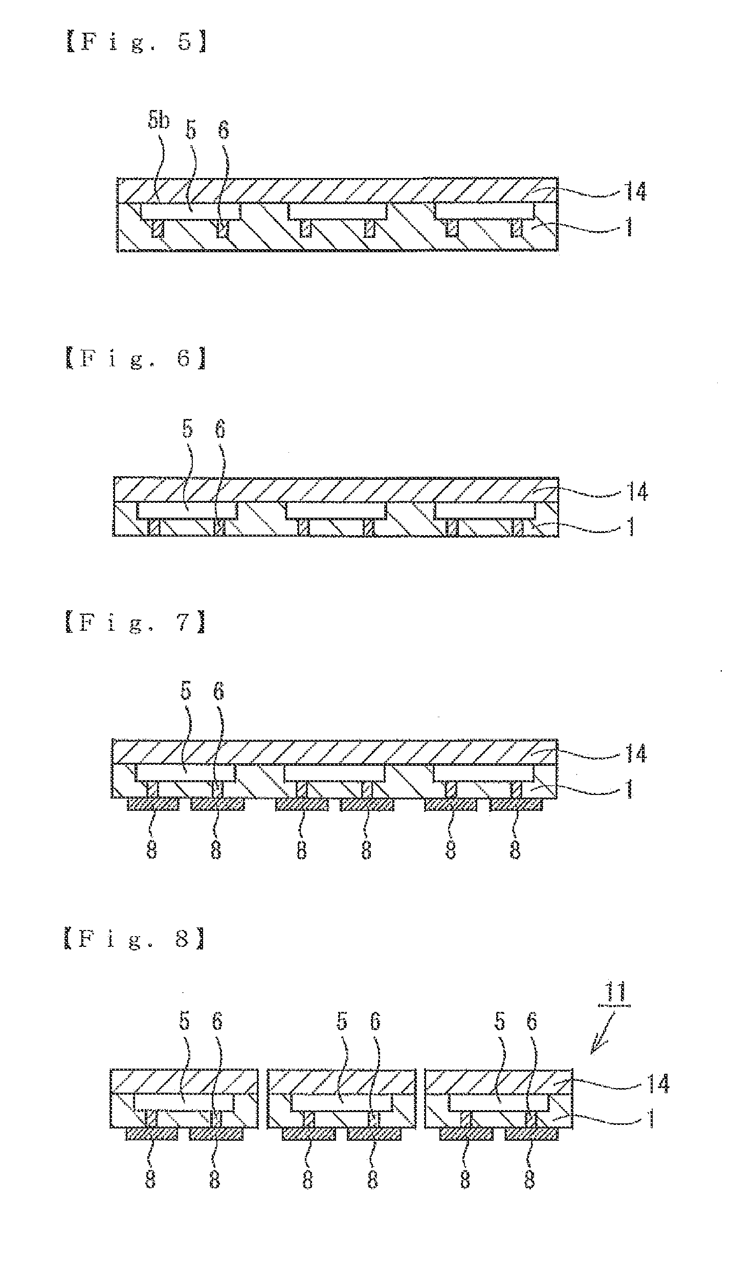
[0125]The case is explained in the above-described first embodiment in which the conductive member 6 is exposed by the face side processing step, in which the surface is ground where the film 14 for a semiconductor backside of the thermosetting resin layer 1 is not pasted to (refer to FIG. 6). However, the method of exposing the conductive member 6 is not limited to this in the present invention, and the conductive member can be also exposed by a laser processing step from the thermosetting resin layer 1 side (a laser processing step). In this case, the laser processing step is performed instead of the face side processing step. FIG. 9 is a schematic sectional view showing a method of manufacturing a semiconductor device according to a second embodiment of the present invention. As shown in FIG. 9, laser processing is performed from the thermosetting resin layer 1 side to expose the conductive member 6 in the second embodiment. A carbon dioxide gas laser, a YAG laser, an excimer las...

third embodiment

[0126]The case is explained in the above-described first embodiment in which the plurality of semiconductor chips 5 are arranged on the thermosetting resin layer 1 and then embedded; that is, the semiconductor chip arranging step (step A) is performed, and then the semiconductor chip embedding step (step B) is performed. However, the method of embedding the semiconductor chips in the thermosetting resin layer is not limited to this in the present invention, and the semiconductor chips can be directly embedded in the thermosetting resin layer one by one. FIG. 10 is a schematic sectional view showing a method of manufacturing a semiconductor device according to a third embodiment of the present invention. As shown in FIG. 10, the semiconductor chips 5 can be directly embedded in the thermosetting resin layer 1 one by one in the third embodiment. A conventionally known flip-chip bonder 22 can be used for embedding. As the embedding conditions, the pressure is preferably 0.01 to 3 MPa, ...

fourth embodiment

[0128]The case is explained in the above-described first embodiment in which a plurality of semiconductor chips 5 are arranged on the thermosetting resin layer 1 so that the thermosetting resin layer 1 and the circuit forming surface 5a of the semiconductor chips 5 are facing each other in the semiconductor chip arranging step (step C) (refer to FIG. 1). However, the arrangement of the semiconductor chips is not limited to this in the present invention, and a plurality of semiconductor chips may be arranged on the thermosetting resin layer so that the thermosetting resin layer and the surface opposite to the circuit forming surface of the semiconductor chips are facing each other. FIGS. 11 and 12 are schematic sectional views showing a method of manufacturing a semiconductor device according to a fourth embodiment of the present invention. As shown in FIG. 11, a plurality of semiconductor chips 5 are arranged on the thermosetting resin layer 1 so that the thermosetting resin layer 1...


PUM


Abstract

The objective of the present invention is to provide a method of manufacturing a semiconductor device having less contamination of a semiconductor chip and good productivity. The present invention is a method of manufacturing a semiconductor device having a semiconductor chip, with the steps of preparing a plurality of semiconductor chips, preparing a resin sheet having a thermosetting resin layer, arranging the plurality of semiconductor chips on the thermosetting resin layer, arranging a cover film on the plurality of semiconductor chips, and embedding the plurality of semiconductor chips in the thermosetting resin layer by a pressure applied through the arranged cover film, in which the contact angle of the cover film to water is 90° or less.

Description

BACKGROUND OF THE INVENTION[0001]1. Field of the Invention[0002]The present invention relates to a method of manufacturing a semiconductor device.[0003]2. Description of the Related Art[0004]In recent years, the miniaturization of semiconductor devices and the refinement of wiring have increasingly advanced, more I / O pads and vias have to be arranged in a narrow region of a semiconductor chip (the overlapping region of a semiconductor chip when the semiconductor chip is being viewed in a planar view), and at the same time the pin density has increased. In addition, a large number of terminals are formed in the semiconductor chip region of a BGA (Ball Grid Array) package, and the region where other elements can be formed is limited. Therefore, a method is pursued of drawing wiring from the terminals to the outside of the semiconductor chip region on the substrate of the semiconductor package.[0005]Under such circumstances, if the miniaturization of semiconductor devices and the refin...

Claims


Application Information

Patent Timeline
IPC IPC(8): H01L21/56
CPCH01L21/56H01L21/561H01L24/96H01L23/3107H01L21/568H01L2924/12042H01L2224/73267H01L2224/04105H01L2924/00
Inventor SHIMIZU, YUSAKUAKIZUKI, SHINYAODA, TAKASHITOYODA, EIJIMATSUMURA, TAKESHI
Owner NITTO DENKO CORP
Why Eureka
Try Eureka