
Structures and manufacturing methods for glass covered electronic devices

a technology of electronic devices and structures, applied in the field of electronic displays, can solve the problems of affecting the orderly arrangement of molecules, affecting the performance of electronic devices, and affecting etc., and achieving the effect of improving the quality of electronic devices, improving the service life and improving the service li

Inactive Publication Date: 2013-07-04
SYNAPTICS INC
View PDF6 Cites 55 Cited by
  • Summary
  • Abstract
  • Description
  • Claims
  • Application Information

AI Technical Summary

Benefits of technology

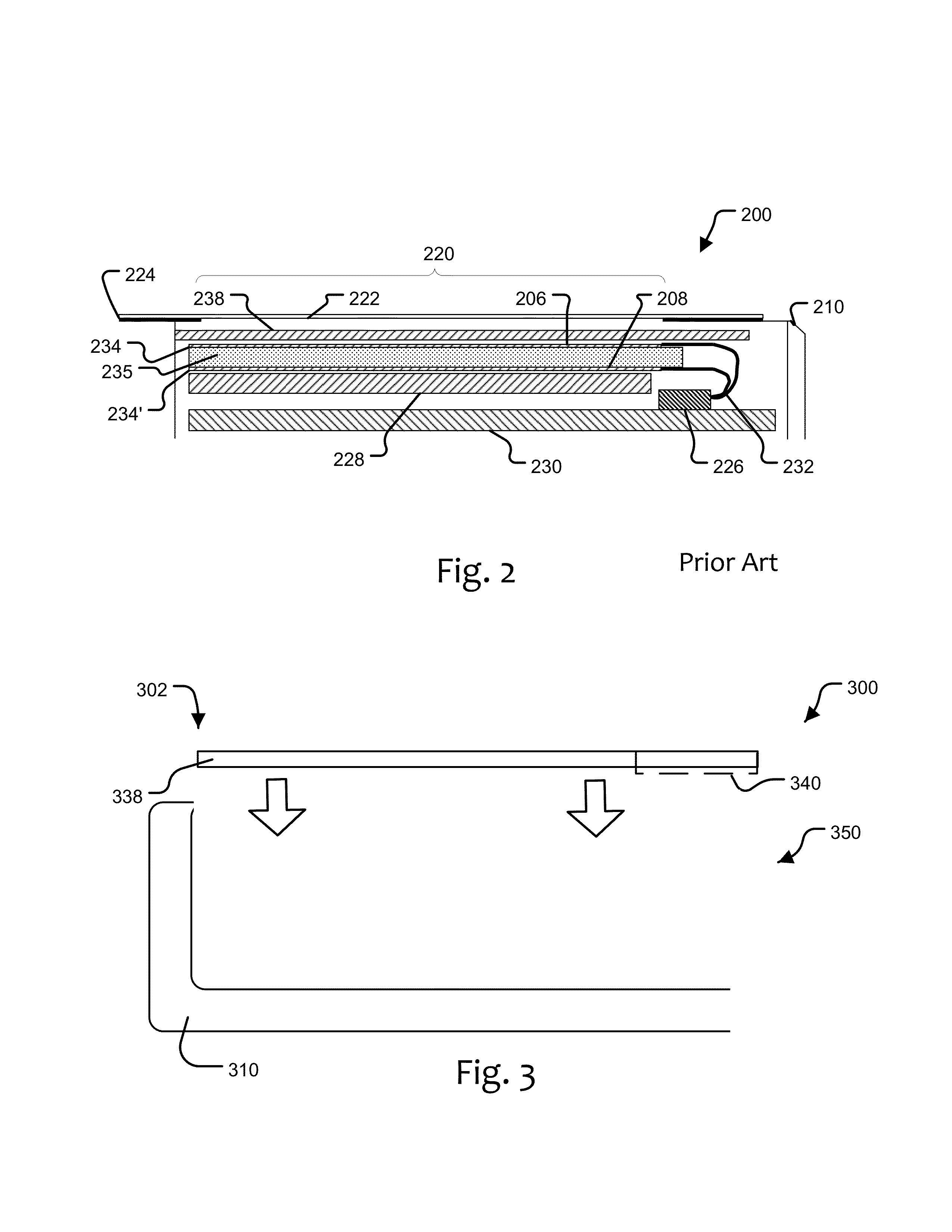
This patent is about electronic device displays and how to make them. The patent describes methods for making displays that are thin, strong, and can withstand damage from impact. The methods involve using a thin glass layer, a clear adhesive layer, a sensor layer, and a base glass layer. The adhesive layer between the thin glass layer and the base glass layer is preferably about 8-mil in thickness or less, and has a hardness of about 80 Shore A or higher. The displays can also have a total thickness of less than 800 micrometers and are constructed to pass a ball drop test of 2 grams at greater than 4 feet. The patent also describes an impact resistant display device that can withstand damage from impact. The sensor layer can communicate with a printed circuit board, storage, memory, a system on a chip, a CPU core, a GPU core, Wi-Fi connectivity, Bluetooth connectivity, camera, audio, battery, power connector, computer readable media, and instructions for operation on computer readable media. The adhesive layer can also have a modulus of greater than 1 GPa. The patent also mentions that the sensor layer can include thin patterned conductive traces.

Problems solved by technology

Voltages applied between the front and back coatings disrupt the orderly arrangement of the molecules sufficiently to darken the liquid and form visible patterns.
One drawback of currently available electronic device interfaces is that the screen can be damaged fairly easily.
This can be particularly problematic for devices that are designed for increased mobility and may be subjected to harsh conditions.

Method used


Image

  • Structures and manufacturing methods for glass covered electronic devices
  • Structures and manufacturing methods for glass covered electronic devices
  • Structures and manufacturing methods for glass covered electronic devices

Examples


Embodiment Construction

I. Devices

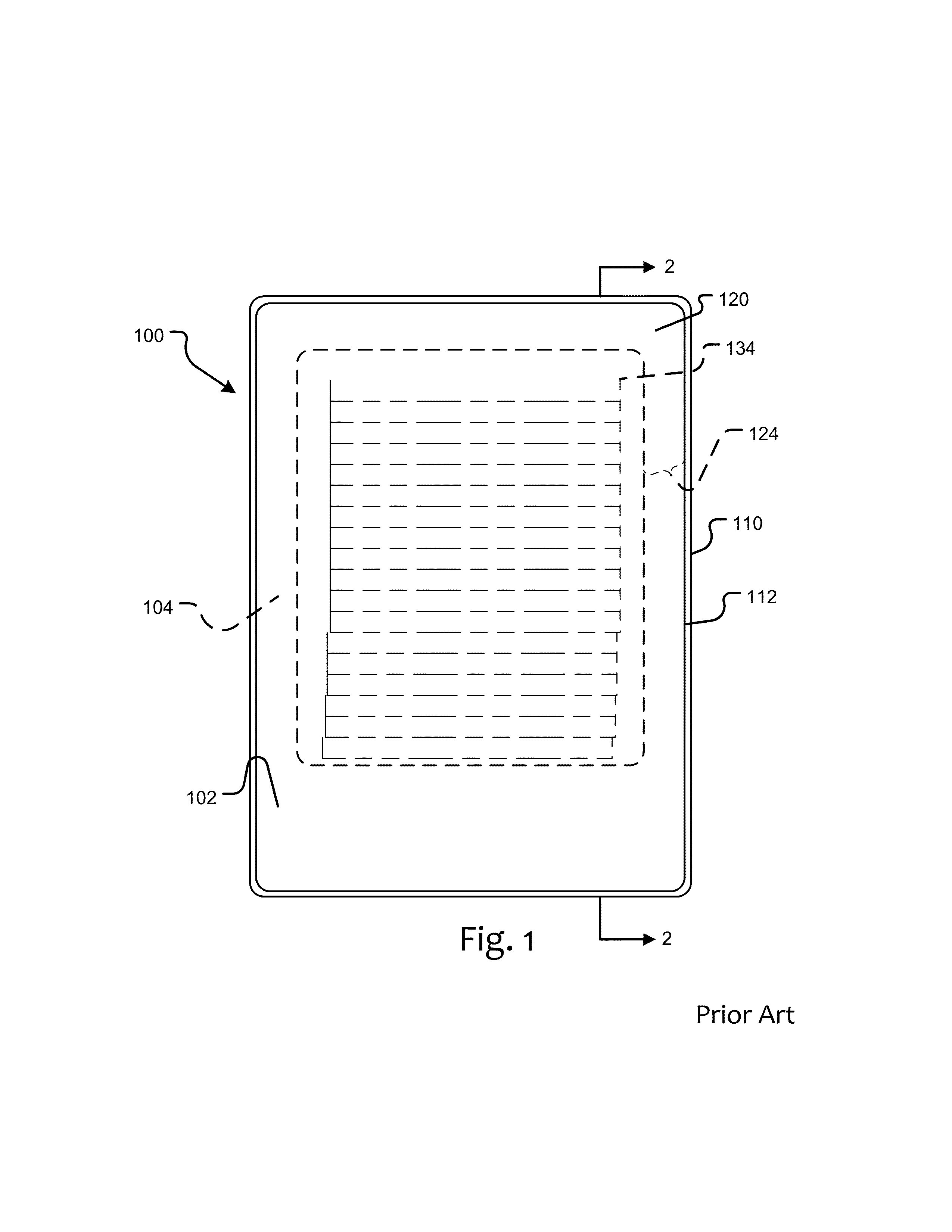
[0026]For purposes of illustration a touch screen display currently employed by, for example, a smart phone is described. Such a touch screen typically comprises a 9 cm (3.5 in)×6 cm (2.4 in) liquid crystal display (LCD) with a scratch-resistant glass layer. Other size touch screens can be employed without departing from the scope of the disclosure.

[0027]The capacitive touch screen of the LCD is typically optimized for a bare finger, or multiple finger multi-touch, sensing. However, as will be appreciated by those skilled in the art, a variety displays as well as a variety of touch screen configurations and touch screen operated devices can be used without departing from the scope of the disclosure.

[0028]An LCD touch screen typically is an assembly that includes an LCD, a printed circuit board (PCB) on which input-output (I / O) connections and integrated circuits (ICs) performing various functions are mounted, a transparent touch screen circuit pattern on a transparent subs...


PUM


Abstract

The disclosure is directed to electronic device displays which are constructed to withstand damage from an impact resistance test wherein a steel ball of 2 g having a diameter of 8 mm is dropped from a designated height greater than 1 ft, more preferably greater than 2 ft, even more preferably greater than 3 ft, still even more preferably greater than 4 ft, yet even more preferably greater than 5 ft and even more preferably greater than 6 ft. The displays are configured using, for example, ultrathin glass adhered to a base glass, wherein the adhesive layer is optimized for thinness and stiffness.

Description

CROSS-REFERENCE[0001]This application claims the benefit of U.S. Provisional Application No. 61 / 582,660, entitled Structure and Manufacturing Methods for Glass Covered Electronic Device by Paul Wickboldt and Eric Jones, filed Jan. 3, 2012, which application is incorporated herein by reference.BACKGROUND OF THE INVENTION[0002]A variety of electronic displays are used with electronic devices. Displays can operate using either emissive (pixels generate light), transmissive (light transmitted through pixels) and reflective (ambient light reflected) approaches. Display types may include, for example, liquid crystal displays (LCDs) which use liquid crystal cells that change transmission, or reflection in an applied electric field, organic light emitting diode (OLED) devices which utilize a light emitting diode (LED) in which an emissive electroluminescent film of organic compounds emits light in response to an electric current, and different types of electrophoretic displays in which pigm...

Claims


Application Information

Patent Timeline
Patent Type & Authority Applications(United States)
IPC IPC(8): G06F3/045
CPCG02B1/105G06F3/045G02F2202/28G02F2001/133331G02F2201/503G02F2001/133311G02F1/133308G02B1/18G02B1/14G02F1/133311G02F1/133331G06F3/041B32B2457/202B32B33/00
Inventor WICKBOLDT, PAULJONES, ERIC
Owner SYNAPTICS INC
Learn More