Method of cutting light-emitting device chip wafer by using laser scribing

a technology of light-emitting devices and laser scribing, which is applied in the manufacture of semiconductor/solid-state devices, semiconductor devices, electrical devices, etc., can solve the problems of electrical cutting process contaminating the environment, contact failure between electrodes and multi-probes, and problems in the light-emitting device chips. achieve the effect of increasing the productivity of the cutting process

Active Publication Date: 2013-07-04
SAMSUNG ELECTRONICS CO LTD
View PDF9 Cites 12 Cited by
  • Summary
  • Abstract
  • Description
  • Claims
  • Application Information

AI Technical Summary

Benefits of technology

[0009]Disclosed are methods of cutting light-emitting device chip wafers to increase the productivity of a cutting process by separating the light-emitting device chips by using a laser scribing process and a breaking process.
[0018]According to the exemplary embodiments, the failure rate of light-emitting device chips may be reduced by reducing particles generated from a cutting process.

Problems solved by technology

However, the mechanical cutting process may contaminate the environment due to dust, generated during the mechanical cutting process.
Also, a contact failure between electrodes and a multi-probe may occur due to a disorder of alignment of the separated light-emitting device chips on the protection tape.
Thus, the contact failure may cause problems in the light-emitting device chips.

Method used


Image

  • Method of cutting light-emitting device chip wafer by using laser scribing
  • Method of cutting light-emitting device chip wafer by using laser scribing
  • Method of cutting light-emitting device chip wafer by using laser scribing

Examples


Embodiment Construction

[0024]Reference will now be made in detail to embodiments, examples of which are illustrated in the accompanying drawings. In the drawings, like reference numerals refer to like elements throughout and the thicknesses or sizes of elements are exaggerated for convenience of explanation and clarity. It will be understood that when an element or layer is referred to as being “on” another element or layer, it can be directly or indirectly formed on the other element or layer. For example, intervening elements or layers may be present.

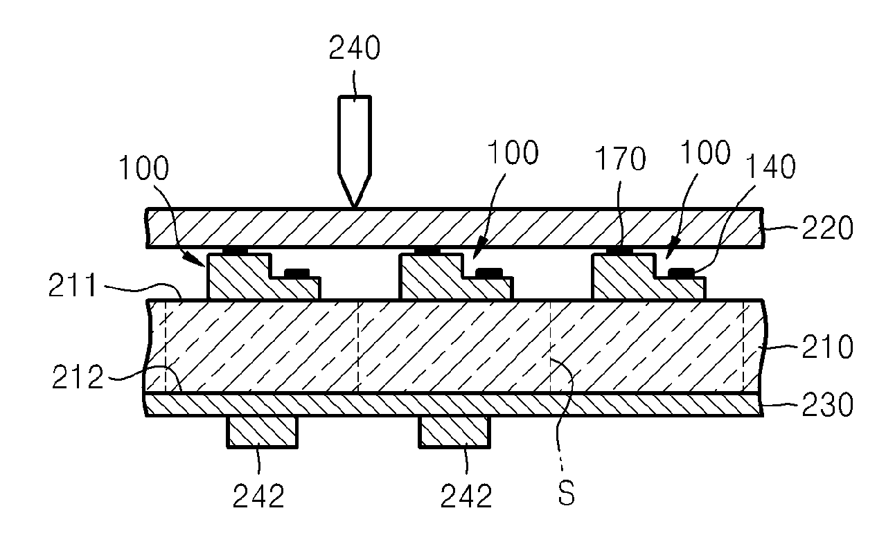
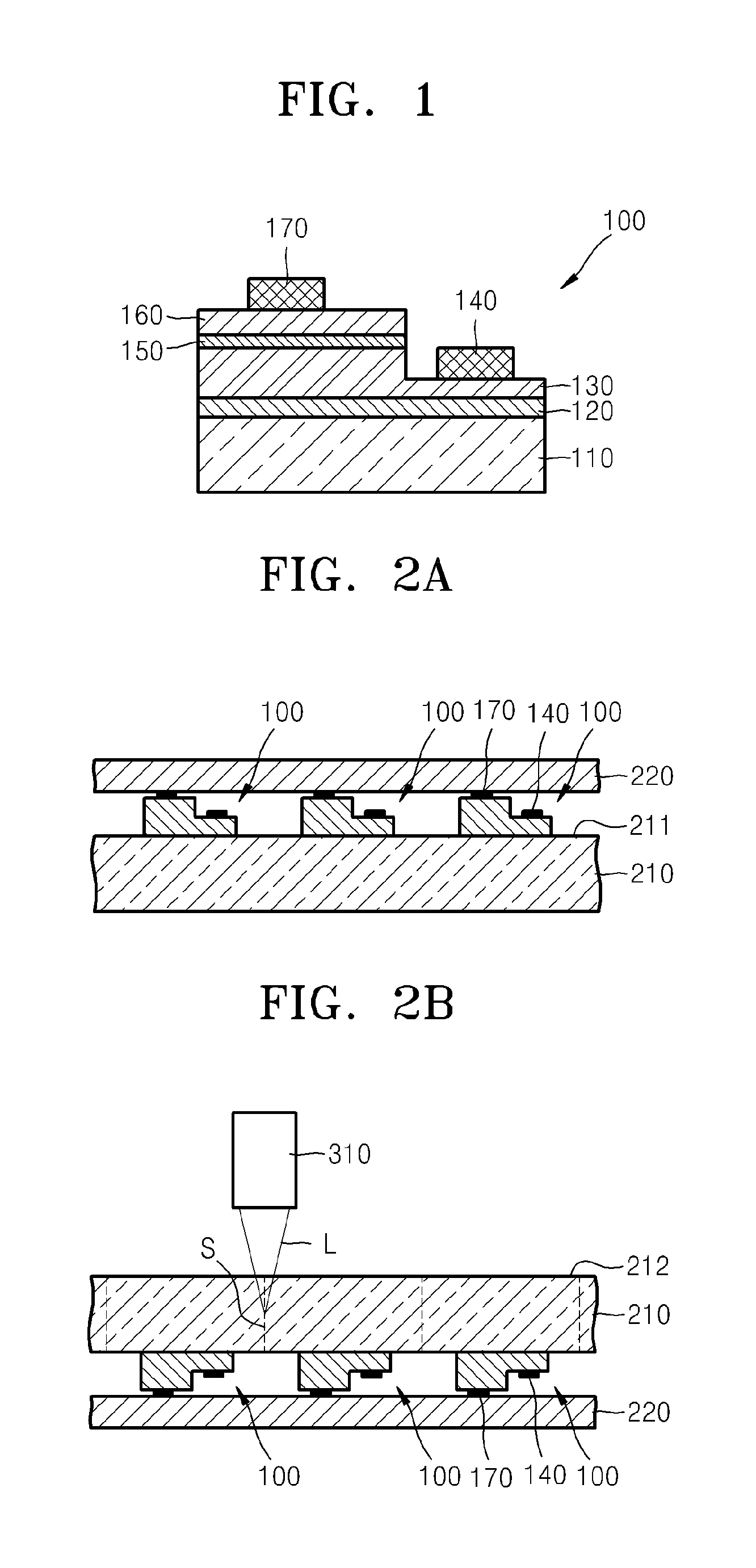
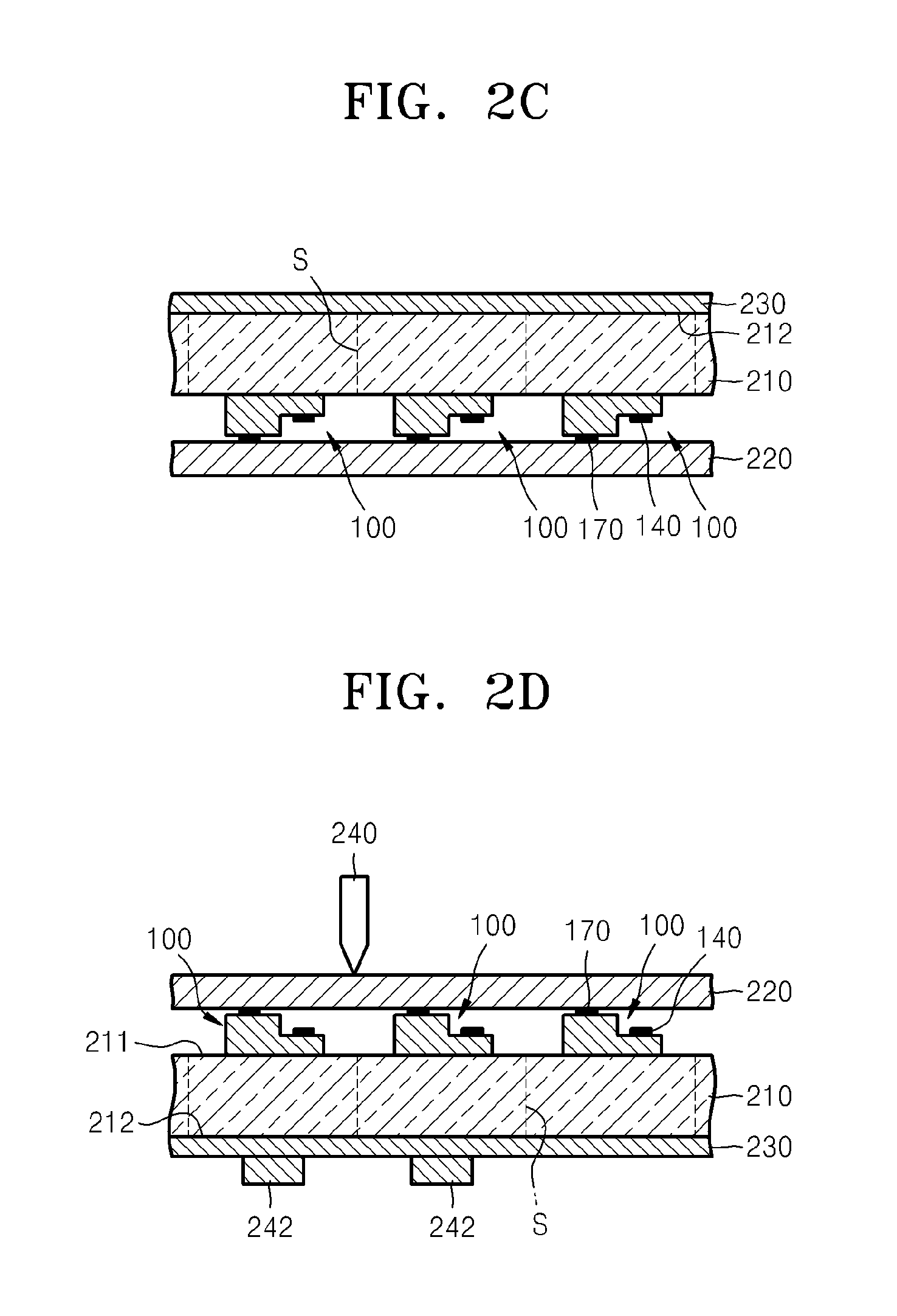
[0025]FIG. 1 is a schematic cross-sectional view of an example of a light-emitting device chip according to an embodiment of the present invention.

[0026]Referring to FIG. 1, a buffer layer 120 is formed on a substrate 110. The substrate 110 may be a sapphire substrate 110. The buffer layer 120 may be formed of InxGayAlzN, ZrB2, HfB2, ZrN, HfN, TiN, or AlN. An n-type nitride layer 130 is formed on the buffer layer 120. The buffer layer 120 is formed to mitig...


PUM


Abstract

Methods of cutting a light-emitting device chip wafer by using a laser scribing process. The method includes: preparing a wafer that has a plurality of semiconductor chips on an upper surface of the wafer; attaching a first tape covering the semiconductor chips to the upper surface of the wafer; forming scribing lines to define each of the semiconductor chips on the wafer by irradiating a laser beam onto a lower surface of the wafer; attaching a second tape to the lower surface of the wafer; and breaking the wafer into a plurality of chips by applying a physical force to the wafer along the scribing lines.

Description

CROSS-REFERENCE TO RELATED APPLICATIONS[0001]This application claims the benefit of Korean Patent Application No. 10-2011-0147417, filed on Dec. 30, 2011, in the Korean Intellectual Property Office, the disclosure of which is incorporated herein in its entirety by reference.BACKGROUND[0002]1. Field[0003]The present disclosure relates to methods of cutting a light-emitting device chip wafer on which a plurality of light-emitting device chips are formed using laser scribing.[0004]2. Description of the Related Art[0005]Light-emitting device chips, e.g., light-emitting diodes (LEDs), are semiconductor devices that realize various light colors by configuring a light source through a PN junction of compound semiconductors. LEDs have a long lifespan, may be miniaturized and manufacture light, and may be driven at a low voltage due to high directionality. Also, LEDs are resilient to impact and vibration, do not require a preheating time and a complicated driving, and may be packaged in vari...

Claims


Application Information

Patent Timeline
Patent Type & Authority Applications(United States)
IPC IPC(8): H01L33/00
CPCH01L33/0095H01L33/007H01L33/00
Inventor JANG, YU-SUNG
Owner SAMSUNG ELECTRONICS CO LTD
Why Eureka
Try Eureka