Processing liquid for suppressing pattern collapse of microstructure, and method for producing microstructure using same
a technology of microstructure and processing liquid, which is applied in the direction of photosensitive material processing, photomechanical equipment, instruments, etc., can solve the problems of resist pattern collapse, pattern collapse, pattern collapse of structure, etc., and achieve the effect of suppressing the pattern collapse of a microstructur
- Summary
- Abstract
- Description
- Claims
- Application Information
AI Technical Summary
Benefits of technology
Problems solved by technology
Method used
Image
Examples
examples
[0034]The present invention will be described in more detail with reference to Examples, etc., below, but the present invention is not limited to these Examples.
[0035]>
[0036]Processing liquids for suppressing pattern collapse of a microstructure were prepared according to the formulation compositions (% by mass) as shown in Table 1.
TABLE 1Number ofcarbon atomsin alkylKindgroup*1ContentProcessingDodecyl pyridinium chloride12500 ppmliquid 1ProcessingDodecyl pyridinium chloride128%liquid 2Processing1-Dodecyl-4-methyl12300 ppmliquid 3pyridinium chlorideProcessing1-Dodecyl-4-methyl1210% liquid 4pyridinium chlorideProcessingTetradecyl pyridinium chloride14100 ppmliquid 5ProcessingTetradecyl pyridinium chloride145%liquid 6Processing1-Tetradecyl-4-methyl14 50 ppmliquid 7pyridinium chlorideProcessing1-Tetradecyl-4-methyl143%liquid 8pyridinium chlorideProcessingHexadecyl pyridinium chloride16 30 ppmliquid 9ProcessingHexadecyl pyridinium chloride161%liquid 10Processing1-Hexadecyl-4-methyl16 10...
examples 1 to 12
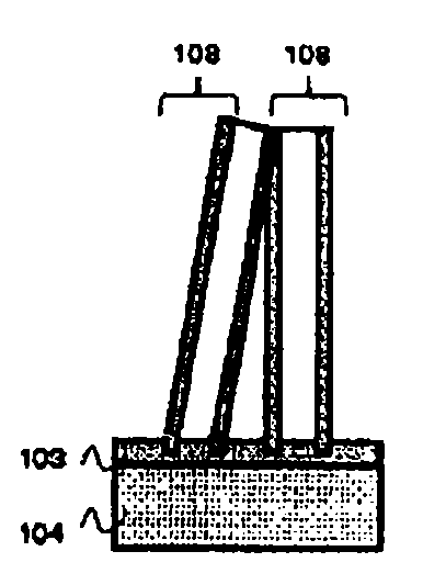
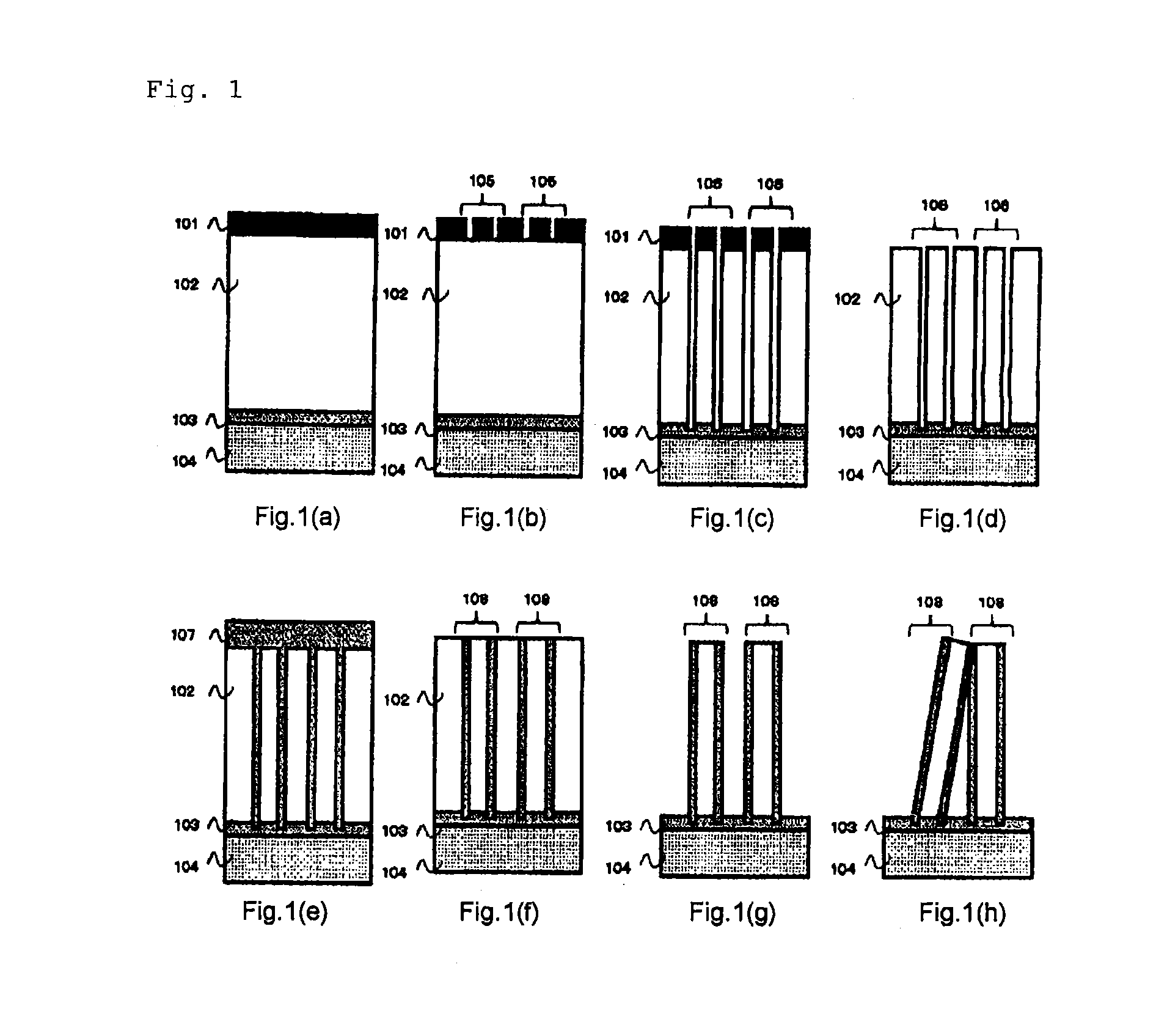
[0037]As shown in FIG. 1(a), silicon nitride 103 (thickness: 100 nm) and silicon oxide 102 (thickness: 1,200 nm) were formed as films on a silicon substrate 104, then a photoresist 101 was formed, and the photoresist 101 was exposed and developed, thereby forming a tubular (chimney-shaped) opening 105 (diameter: 125 nm, distance between circles: 50 nm), as shown in FIG. 1(b). The silicon oxide 102 was etched by dry etching with the photoresist 101 as a mask, thereby forming a cylindrical hole 106 reaching the layer of silicon nitride 103, as shown in FIG. 1(c). The photoresist 101 was then removed by asking, thereby providing a structure having the silicon oxide 102 with the cylindrical hole 106 reaching the layer of silicon nitride 103, as shown in FIG. 1(d). The cylindrical hole 106 of the resulting structure was filled and deposited with polysilicon 107 (FIG. 1(e)), and an excessive portion of the polysilicon 107 on the silicon oxide 102 was removed by chemical mechanical polishi...
PUM
 Abstract
Description
Claims
Application Information

