Treatment liquid for inhibiting pattern collapse in microstructures, and microstructure manufacturing method using said treatment liquid

a technology of treatment liquid and pattern collapse, which is applied in the direction of detergent compositions, photomechanical devices, instruments, etc., can solve problems such as pattern collapse, resist pattern collapse, and pattern collapse of structure, and achieve the effect of reducing the number of resist patterns

Active Publication Date: 2013-06-27
MITSUBISHI GAS CHEM CO INC
View PDF3 Cites 7 Cited by
  • Summary
  • Abstract
  • Description
  • Claims
  • Application Information

AI Technical Summary

Benefits of technology

[0024]According to the present invention, there are provided a processing liquid that is capable of suppressing pattern collapse of a microstructure formed of silicon oxide, such as a semiconductor device and a micromachine, and a method for producing a microstructure using the processing liquid.

Problems solved by technology

However, the progress of miniaturization of the resist pattern causes pattern collapse as a major problem.
It has been known that upon drying the resist pattern to remove a processing liquid used in wet processing (which is mainly a rinsing treatment for washing away a developer solution) therefrom after developing the resist pattern, the collapse of the resist pattern is caused by the stress derived by the surface tension of the processing liquid.
However, associated. with the progress of reduction of size, increase of integration degree and increase of speed of a semiconductor device and a micromachine, the pattern collapse of the structure is becoming a major problem due to miniaturization and increase of aspect ratio of the pattern.

Method used


Image

  • Treatment liquid for inhibiting pattern collapse in microstructures, and microstructure manufacturing method using said treatment liquid
  • Treatment liquid for inhibiting pattern collapse in microstructures, and microstructure manufacturing method using said treatment liquid

Examples


examples

[0044]The present invention will be described in more detail with reference to Examples, etc., below, but the present invention is not limited to these Examples.

[0045]>

[0046]Processing liquids for suppressing pattern collapse of a microstructure were prepared according to the formulation compositions (% by mass) as shown in Table 1.

TABLE 1Number ofcarbon atomsin alkylKindgroup*1ContentProcessing1-Dodecyl-3-methyl125%liquid 1imidazolium chlorideProcessing1-Tetradecyl-3-methyl14500 ppmliquid 2imidazolium chlorideProcessing1-Hexadecyl-3-methyl16100 ppmliquid 3imidazolium chlorideProcessingTetradecyl pyridinium chloride1410% liquid 4Processing1-Tetradecyl-4-methyl141,000 ppm  liquid 5pyridinium chlorideProcessingHexadecyl pyridinium chloride16300 ppmliquid 6Processing1-Hexadecyl-4-methyl16 50 ppmliquid 7pyridinium chlorideProcessingHexadecyl trimethyl161%liquid 8ammonium chlorideProcessingBenzyl dimethyl hexadecyl163,000 ppm  liquid 9ammonium chlorideProcessingOctadecyl trimethyl18200 p...

examples 1 to 11

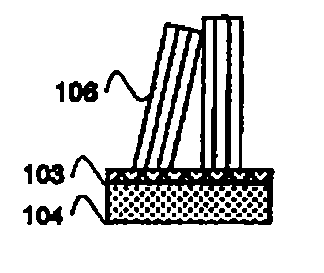
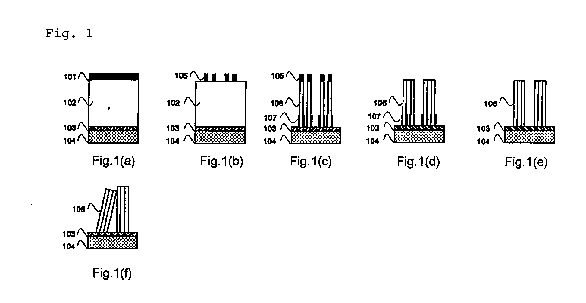
[0047]As shown in FIG. 1(a), silicon nitride 103 (thickness: 100 nm) and silicon oxide 102 (thickness: 1,200 nm) were formed as films on a silicon substrate 104, then a photoresist 101 was formed, and the photoresist 101 was exposed and developed, thereby forming a tubular (chimney-shaped) photoresist 105 (diameter: 125 nm, distance between circles: 50 nm), as shown in FIG. 1(b). The silicon oxide 102 was etched. by dry etching with the photoresist 105 as a mask, thereby forming a cylindrical hollow 106 reaching the layer of silicon nitride 103, as shown in FIG. 1(c). Upon the dry etching, etching residues 107 remained both inside and outside of the cylindrical hollow. The photoresist 105 was then removed by ashing, thereby providing a structure with the cylindrical hollow 106 formed of silicon oxide and reaching the layer of silicon nitride 103, as shown in FIG. 1(d). The etching residues 107 of the resulting structure were removed by dissolving with a 0.1 wt % hydrofluoric acid aq...


PUM

PropertyMeasurementUnit
contact angleaaaaaaaaaa
aspect ratioaaaaaaaaaa

Abstract

There are provided a processing liquid for suppressing pattern collapse of a microstructure which includes at least one compound selected from the group consisting of an imidazolium halide containing an alkyl group having 12, 14 or 16 carbon atoms, a pyridinium halide containing an alkyl group having 14 or 16 carbon atoms and an ammonium halide containing an alkyl group having 16 or 18 carbon atoms, and water; and a method for producing a microstructure formed of silicon oxide using the processing liquid.

Description

TECHNICAL FIELD[0001]The present invention relates to a processing liquid for suppressing pattern collapse of a microstructure, and a method for producing a microstructure using the processing liquid.BACKGROUND ART[0002]The photolithography technique has been employed as a formation and processing method of a device having a microstructure used in a wide range of fields of art including a semiconductor device, a circuit board and the like. In these fields of art, reduction of size, increase of integration degree and increase of speed of a semiconductor device considerably proceed associated with the highly sophisticated demands on capabilities, which bring about continuous miniaturization and increase of aspect ratio of a resist pattern used for photolithography. However, the progress of miniaturization of the resist pattern causes pattern collapse as a major problem.[0003]It has been known that upon drying the resist pattern to remove a processing liquid used in wet processing (whi...

Claims


Application Information

Patent Timeline
Patent Type & Authority Applications(United States)
IPC IPC(8): C11D7/32
CPCB81C1/00825C11D7/3281C11D7/3209H01L21/0206G03F7/425H01L21/0274
Inventor MATSUNAGA, HIROSHIOHTO, MASARU
Owner MITSUBISHI GAS CHEM CO INC
Why Eureka
Try Eureka