Treatment liquid for inhibiting pattern collapse in microstructures, and microstructure manufacturing method using said treatment liquid
a technology of treatment liquid and pattern collapse, which is applied in the field of processing liquid, can solve problems such as pattern collapse, resist pattern collapse, pattern collapse,
- Summary
- Abstract
- Description
- Claims
- Application Information
AI Technical Summary
Benefits of technology
Problems solved by technology
Method used
Image
Examples
examples
[0040]The present invention will be described in more detail with reference to Examples, etc., below, but the present invention is not limited to these Examples.
[0041]>
[0042]Processing liquids for suppressing pattern collapse of a microstructure were prepared according to the formulation compositions (% by mass) as shown in Table 1.
TABLE 1KindContentProcessing liquid 1Surflon S-221*1 5%Processing liquid 2Surflon S-221*12,000 ppmProcessing liquid 3Surflon S-221*1 10 ppmProcessing liquid 4Surflon S-231*210%Processing liquid 5Surflon S-231*21,000 ppmProcessing liquid 6Surflon S-231*2 100 ppmProcessing liquid 7Surflon S-241*330%Processing liquid 8Surflon S-241*35,000 ppmProcessing liquid 9Surflon S-241*3 50 ppm*1“Surflon S-221” (tradename) available from AGC Seimi Chemical Co., Ltd.; perfluoroalkyl trialkyl ammonium halide (number of carbon atoms in alkyl group: 6); specific gravity: 1.07 (25° C.); viscosity: 6.7 mPa · s (25° C.); pH: 8.0 to 10.0; surface tension: 15.8 mN / m (0.1% aqu...
examples 1 to 9
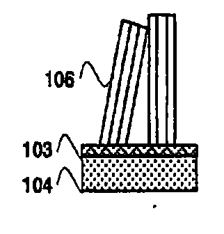
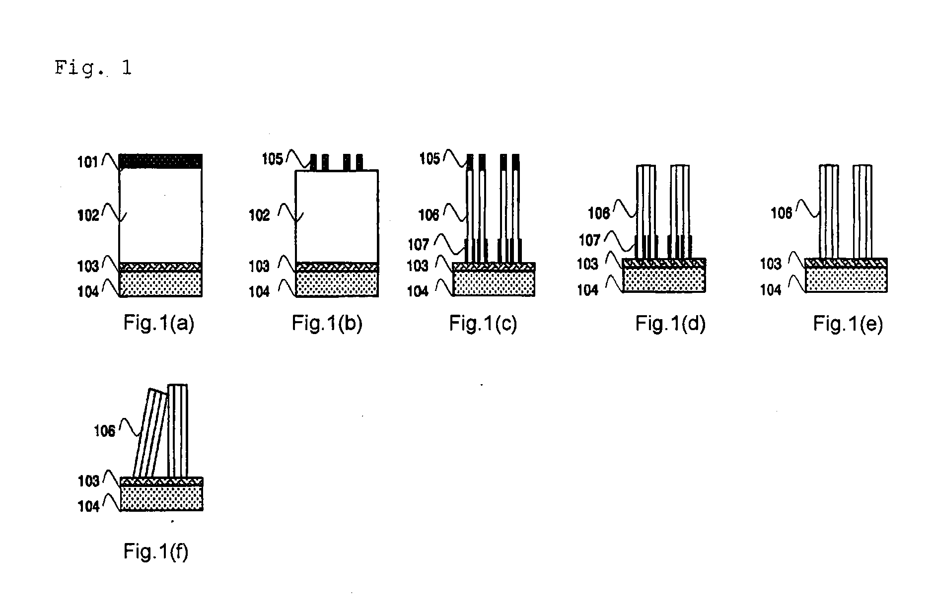
[0043]As shown in FIG. 1(a), silicon nitride 103 (thickness: 100 nm) and silicon oxide 102 (thickness: 1,200 nm) were formed as films on a silicon substrate 104, then a photoresist 101 was formed, and the photoresist 101 was exposed and developed, thereby forming a tubular (chimney-shaped) photoresist 105 (diameter: 125 nm, distance between circles: 50 nm), as shown in FIG. 1(b). The silicon oxide 102 was etched by dry etching with the photoresist 105 as a mask, thereby forming a cylindrical hollow 106 reaching the layer of silicon nitride 103, as shown in FIG. 1(c). Upon the dry etching, etching residues 107 remained both inside and outside of the cylindrical hollow. The photoresist 105 was then removed by ashing, thereby providing a structure having the silicon oxide 102 with the cylindrical hollow 106 reaching the layer of silicon nitride 103, as shown in FIG. 1(d). The etching residues 107 of the resulting structure were removed by dissolving with a 0.1 wt % hydrofluoric acid aq...
PUM
 Abstract
Description
Claims
Application Information

