Semiconductor device and manufacturing method thereof

a semiconductor and manufacturing method technology, applied in the direction of semiconductor devices, electrical appliances, transistors, etc., can solve the problems of reducing the threshold voltage (vt) of the transistor, increasing the subthreshold current and reducing the threshold voltage of the transistor, and affecting capacitors, etc., to achieve the effect of convenient manufacturing and facilitate the formation of bit lines

Inactive Publication Date: 2013-07-18
LONGITUDE LICENSING LTD
View PDF2 Cites 20 Cited by
  • Summary
  • Abstract
  • Description
  • Claims
  • Application Information

AI Technical Summary

Benefits of technology

[0016]Thus, there is a demand for a semiconductor device that is capable of ensuring sufficient transistor ON current while avoiding operational interference between adjacent transistors, and thus resolving the problem of difficulty in manufacturing, even if the semiconductor device is a DRAM having transistors with trenches. There is also a demand for a manufacturing method of such a semiconductor device.
[0018]In the semiconductor device of the invention, the semiconductor substrate is provided with a first impurity diffusion region covering the top part of the gate insulating film disposed on the first side face, a second impurity diffusion region at least covering the gate insulating film disposed on the second side face, and a fin formed such that a part of the active region protrudes from the bottom of the gate electrode trench. In this configuration, channel regions are formed on the two surfaces of the bottom of the gate electrode trench and the lower part of the first side face, and on the fin, whereby it is made possible to reduce the channel resistance in comparison with a related semiconductor device in which channel regions are formed on the three surfaces of the bottom and the opposing side faces of the gate electrode trench. This makes it possible to ensure sufficient ON current of transistors.
[0020]Further, the gate electrode is formed to fill the lower part of the gate electrode trench and to stride over the fin via the gate insulating film, and the embedded insulating film is formed to fill the gate electrode trench and cover the top face of the gate electrode, whereby the gate electrode will not protrude above the surface of the semiconductor substrate. This facilitates the formation of a bit line and a capacitor in a later step when the semiconductor device is DRAM, and thus the semiconductor device can be easily manufactured.

Problems solved by technology

When the transistor gate length of a transistor is reduced, the short channel effect in the transistor becomes pronounced, and problems arise of increased subthreshold current and reduced threshold voltage (Vt) of the transistor.
Therefore, when DRAM (Dynamic Random Access Memory) is used as a semiconductor device and a DRAM memory cell is miniaturized, degradation of refresh characteristics poses a serious problem.
The inventor has found that if the size of a transistor configured as described above is further reduced, sufficient ON current cannot be obtained for the transistor, and hence the DRAM becomes difficult to operate normally.
Further, another problem has been revealed that if the trench gate arrangement pitch is reduced, operation of one transistor will interfere with operation of another transistor adjacent thereto, and thus independent operation of the transistors becomes impossible.
It is believed that this problem is also attributable to the fact that a channel region is formed between the trench gates.
The projected gate electrode itself makes it extremely difficult to form bit wiring and a capacitor in later steps.
This poses a problem that manufacturing of a DRAM itself becomes difficult.

Method used


Image

  • Semiconductor device and manufacturing method thereof
  • Semiconductor device and manufacturing method thereof
  • Semiconductor device and manufacturing method thereof

Examples


Embodiment Construction

[0039]The invention will be now described herein with reference to illustrative embodiments. Those skilled in the art will recognize that many alternative embodiments can be accomplished using the teachings of the present invention and that the invention is not limited to the embodiments illustrated for explanatory purposes.

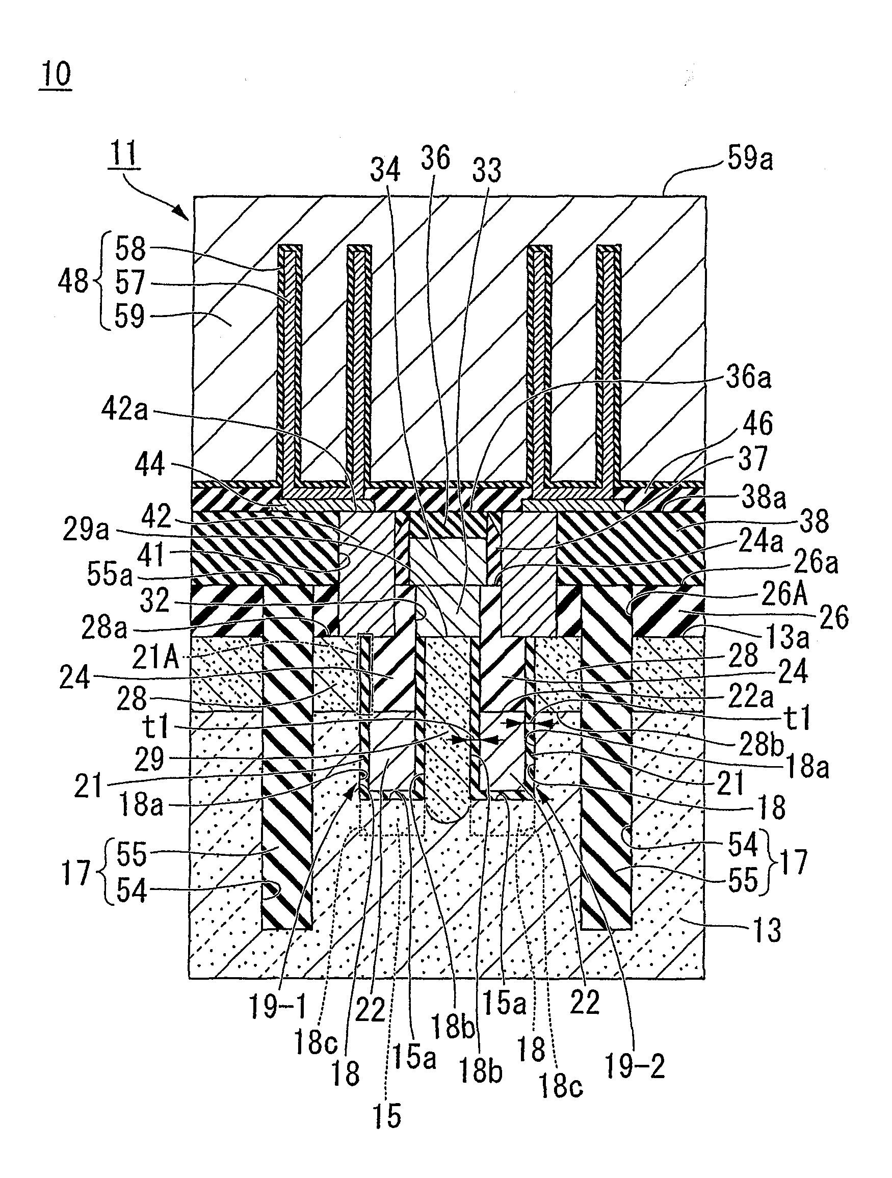
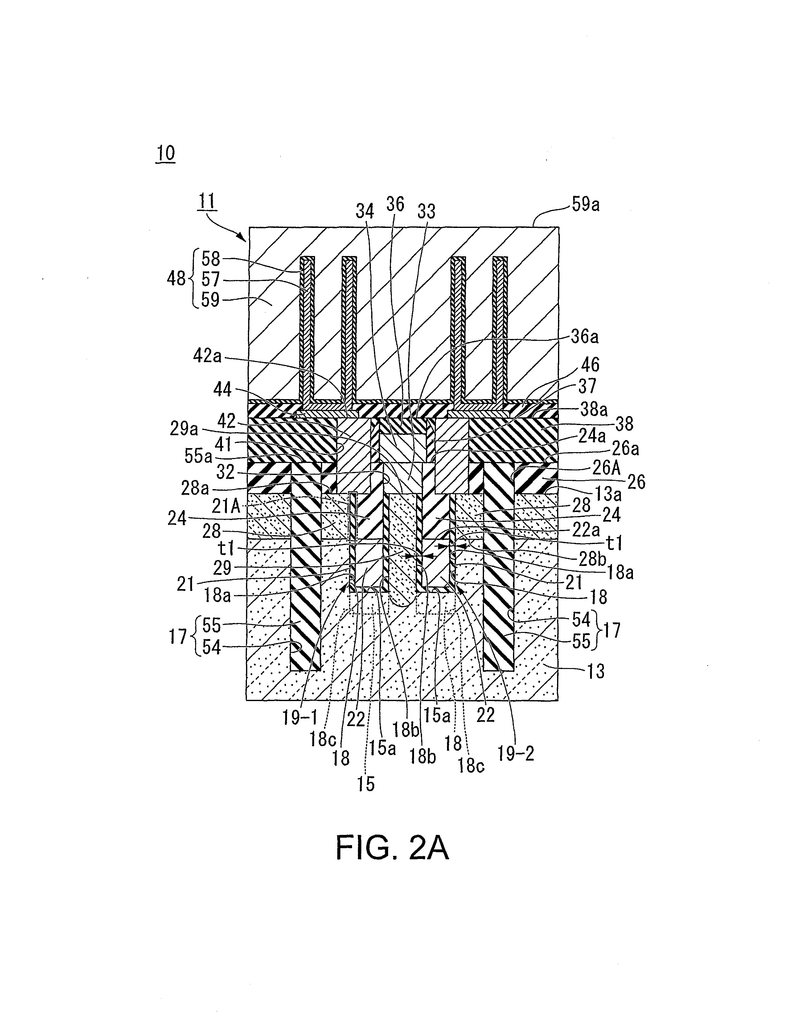
[0040]The inventor obtained a new finding that as a DRAM (Dynamic Random Access Memory) memory cell is miniaturized, a distance between two adjacent cells provided in an active region is reduced, which will cause a disturb failure between the two adjacent cells (hereafter, referred to simply as the disturb failure) in which when one of the cells stores data “0” while the other stores data “1” and the cell storing data “0” is accessed successively, the data stored in the cell storing data “1” will be corrupted. This disturb failure will incur a risk of impairing the reliability of the semiconductor device.

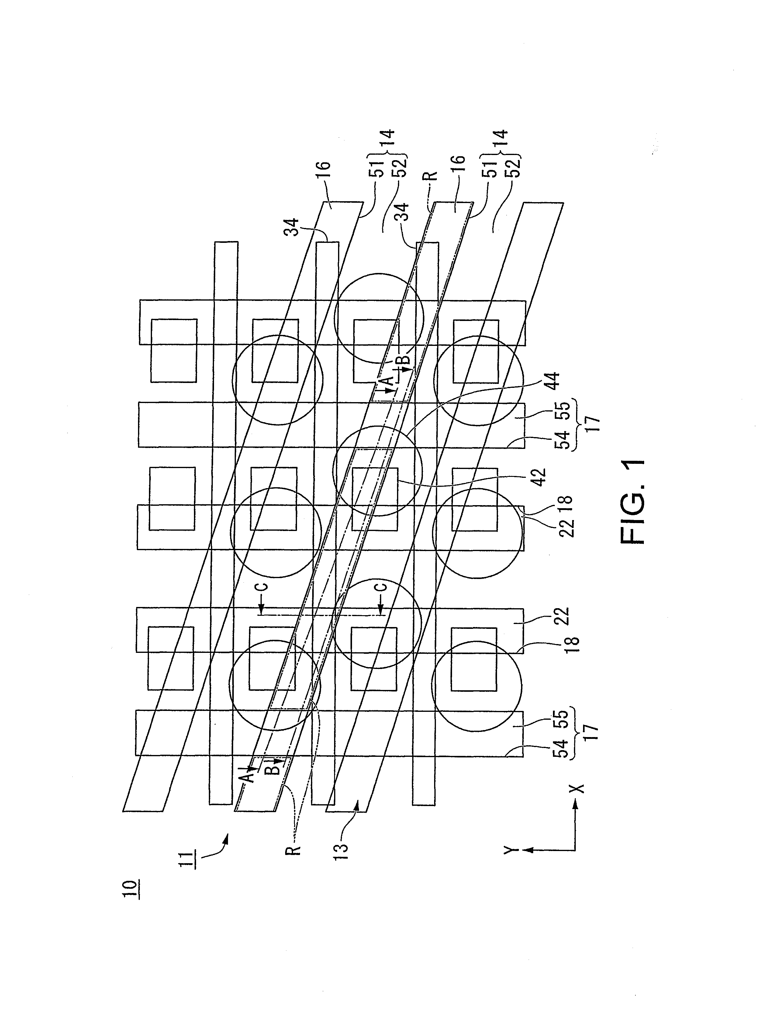
[0041]FIG. 15 is a plan view showing an example of a DRAM l...


PUM


Abstract

A semiconductor device capable of increasing ON current while reducing channel resistance and allowing transistors to operate independently and stably, having a fin formed to protrude from the bottom of a gate electrode trench, a gate insulating film covering the surfaces of the gate electrode trench and the fin, a gate electrode embedded in a lower part of the gate electrode trench and formed to stride over the fin via the gate insulating film, a first impurity diffusion region arranged on a first side face, and a second impurity diffusion region arranged on a second side face.

Description

[0001]This application is based upon and claims the benefit of priority from Japanese Patent Application No. 2012-007445, filed on Jan. 17, 2012, the disclosure of which is incorporated herein in its entirety by reference.BACKGROUND OF THE INVENTION[0002]1. Field of the Invention[0003]This invention relates to a semiconductor device and a manufacturing method of a semiconductor device.[0004]2. Description of the Related Art[0005]In recent years, miniaturization of semiconductor devices such as DRAM (Dynamic Random Access Memory) has been pursued. When the transistor gate length of a transistor is reduced, the short channel effect in the transistor becomes pronounced, and problems arise of increased subthreshold current and reduced threshold voltage (Vt) of the transistor.[0006]Further, if the impurity concentration in a semiconductor substrate is increased in order to suppress drop of the transistor threshold voltage (Vt), joint leak current will be increased.[0007]Therefore, when D...

Claims


Application Information

Patent Timeline
Patent Type & Authority Applications(United States)
IPC IPC(8): H01L27/108H01L29/78
CPCH01L27/10823H01L29/7827H01L29/1037H01L29/4236H01L27/10876H01L29/66621H01L29/78H01L29/0847H01L29/42368H10B12/34H10B12/053
Inventor OYU, KIYONORIOKONOGI, KENSUKEMORI, KAZUTO
Owner LONGITUDE LICENSING LTD
Why Eureka
Try Eureka